
AI-Based Semiconductor Failure Analysis Market Insights
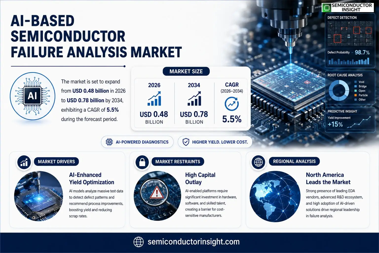
AI-Based Semiconductor Failure Analysis market size was valued at USD 0.45 billion in 2025. The market is set to expand from USD 0.48 billion in 2026 to USD 0.78 billion by 2034, exhibiting a CAGR of 5.5% during the forecast period.
AI‑Based Semiconductor Failure Analysis refers to the application of machine‑learning models and computer‑vision techniques that automatically detect, classify and diagnose defects within integrated circuits during testing or post‑production inspection, thereby accelerating root‑cause identification and yield improvement.The acceleration stems from rising demand for high‑performance chips in data‑center and automotive applications, coupled with mounting pressure on manufacturers to shorten time‑to‑market while preserving yield quality. In March 2024, Synopsys partnered with NVIDIA to integrate GPU‑accelerated inference engines into its failure analysis suite, illustrating how leading vendors are embedding AI capabilities into traditional diagnostic workflows.
MARKET DRIVERS
AI‑Enhanced Yield Optimization
AI-Based Semiconductor Failure Analysis Market is being propelled by manufacturers’ need to shrink cycle times while maintaining high yield. Advanced machine‑learning models ingest terabytes of test‑data, isolate defect patterns, and recommend process tweaks within hoursa timeline that traditional statistical methods cannot match. This capability translates directly into reduced scrap rates and higher throughput, compelling fabs to invest in AI‑driven diagnostic suites.
Regulatory Pressure for Reliability
Stringent reliability standards in automotive and aerospace sectors are forcing chip makers to demonstrate defect‑free performance across longer lifespans. AI algorithms can continuously monitor wafer‑level anomalies, flagging out‑of‑spec events before they propagate to final products. The resulting traceability not only satisfies compliance audits but also strengthens brand reputation, making AI‑based analysis a competitive differentiator.
➤ Producers who embed predictive analytics into their failure‑analysis workflows report up to a 15 % improvement in first‑pass yield, unlocking incremental revenue streams without expanding capacity.
Beyond yield and compliance, the shift toward heterogeneous integrationstacking dies, sensors, and opticscreates new failure modes that are difficult to diagnose with legacy tools. AI’s ability to correlate cross‑layer signals and generate root‑cause hypotheses accelerates the debugging of these complex architectures, reinforcing the strategic importance of AI-Based Semiconductor Failure Analysis Market across emerging form factors.
MARKET CHALLENGES
Data Scarcity and Quality
Effective AI models demand extensive, high‑quality datasets. In many fabs, historical failure logs are fragmented across legacy systems, hindering the creation of comprehensive training corpora. The resulting data gaps force analysts to supplement AI outputs with manual verification, eroding the efficiency gains that the technology promises.
Other Challenges
Talent Gap
The convergence of semiconductor physics and data science requires a rare skill set. Companies often find themselves competing for a limited pool of engineers who understand both silicon defect mechanisms and sophisticated machine‑learning pipelines, which can delay implementation timelines.
Integration Complexity
Legacy failure‑analysis equipment is seldom built with open APIs, making seamless integration of AI modules an engineering challenge. The need for bespoke middleware can inflate project budgets and extend rollout periods, especially for small‑to‑mid‑size players.
MARKET RESTRAINTS
High Capital Outlay
Acquiring AI‑enabled inspection platforms involves significant upfront investment in hardware, software licenses, and workforce training. For fabs operating on thin margins, the cost barrier can postpone adoption until ROI becomes unequivocally demonstrable, tempering market expansion in the short term.
Intellectual Property Concerns
Embedding AI engines within proprietary process flows raises questions about data ownership and algorithmic confidentiality. Companies wary of exposing sensitive yield data to third‑party vendors may limit the scope of AI deployment, thereby constraining the overall market potential.
MARKET OPPORTUNITIES
Edge‑AI Integration for Real‑Time Diagnostics
The emergence of edge‑computing chips that incorporate on‑device AI inference opens a pathway for real‑time failure detection directly on the production line. By processing sensor data at the source, manufacturers can trigger immediate corrective actions, reducing downtime and enabling a closed‑loop quality system. This convergence creates a lucrative niche for vendors that can marry edge hardware with sophisticated failure‑analysis algorithms.
Service‑Based Models for SMEs
Small and medium‑size semiconductor firms are increasingly turning to subscription‑based analytics platforms to avoid the capital intensity of in‑house solutions. Flexible, pay‑as‑you‑go offerings lower the entry threshold and allow these players to benefit from AI insights without large‑scale infrastructure commitments, expanding the addressable base of AI-Based Semiconductor Failure Analysis Market.
AI-Based Semiconductor Failure Analysis Market Trends
AI Integration Accelerates Failure Diagnosis
The infusion of machine‑learning engines into defect detection workflows is reshaping how manufacturers pinpoint yield loss. A recent collaboration between a leading EDA vendor and a GPU specialist introduced real‑time inference directly into failure‑analysis suites, slashing the diagnostic cycle from hours to minutes. This shift is fueled by the surge in high‑performance chips required for data‑center accelerators and next‑generation vehicle control units, where any silicon defect translates into costly downtime. Companies that embed AI into their inspection pipelines now enjoy tighter feedback loops, enabling engineers to apply corrective actions before a batch reaches the market. The ripple effect is a more disciplined design‑for‑manufacturability culture that privileges data‑driven root‑cause analysis over manual microscopy.
Other Trends
Edge Computing and Yield Management
As edge nodes proliferate, the tolerance for defective silicon narrows dramatically. Manufacturers are turning to AI‑enhanced visual inspection to flag sub‑micron anomalies that were previously invisible to conventional test rigs. By correlating defect signatures with process parameters, factories can adjust lithography settings on the fly, preserving yield while accommodating the tighter power and thermal envelopes demanded by edge deployments. The practical outcome is a reduction in scrap rates and a more predictable supply chain for OEMs counting on rapid product refresh cycles.
Predictive Maintenance Through Defect Analytics
Beyond immediate failure detection, the market is witnessing a transition toward anticipatory maintenance models. Historical defect logs, when fed into deep‑learning classifiers, reveal subtle wear patterns that precede catastrophic failure in mature process nodes. Plant operators are leveraging these insights to schedule equipment recalibration before yield degradation becomes apparent, converting what was once a reactive cost center into a strategic asset. This evolution not only protects profit margins but also aligns with broader sustainability goals by minimizing resource waste associated with re‑working or discarding faulty wafers.
COMPETITIVE LANDSCAPEKey Industry Players
Competitive Dynamics Shaping AI‑Driven Failure Analysis
Synopsys anchors the market with its AI‑enhanced failure‑analysis suite, especially after the March 2024 alliance with NVIDIA that placed GPU‑accelerated inference directly into defect‑diagnosis workflows. This partnership illustrates how the traditional EDA stronghold is being reinforced by deep‑learning capability, allowing customers to reduce root‑cause cycles and protect yield on high‑performance chips. Alongside Synopsys, Cadence Design Systems and Mentor, now part of Siemens, supply complementary AI‑augmented verification tools, creating a duopoly where integration depth and platform openness determine client stickiness. The broader supply chain sees heavyweight semiconductor equipment makersApplied Materials, KLA Corporation, and ASMLembedding vision‑based inspection modules that feed real‑time defect data into the same AI models, blurring the line between design‑time analysis and fab‑floor quality control.Beyond the entrenched tier, a constellation of niche players adds differentiation. Advantest and Teradyne leverage AI within automated test equipment to surface defect signatures that traditional probing misses, while Keysight Technologies supplies high‑precision measurement platforms that feed calibrated data to machine‑learning pipelines. Intel and Qualcomm have launched internal AI‑driven yield analytics units, signaling a move toward self‑sufficiency that pressures external vendors to innovate faster. Meanwhile, smaller firms such as DeepVision, InspectAI, and Airo Systems specialize in computer‑vision algorithms for wafer‑level inspection, attracting design houses that require rapid “plug‑and‑play” solutions without the overhead of full‑suite EDA contracts.
List of Key AI-Based Semiconductor Failure Analysis Companies Profiled
- Synopsys
- Cadence Design Systems
- Mentor, a Siemens Business
- NVIDIA
- Applied Materials
- KLA Corporation
- ASML
- Keysight Technologies
- Intel
- Qualcomm
- Advantest
- Teradyne
- DeepVision
- InspectAI
- Airo Systems
Segment Analysis:
| Segment Category | Sub-Segments | Key Insights |
| By Type |
|
Machine‑Learning‑Based Diagnostics
|
| By Application |
|
Automotive Electronics Reliability
|
| By End User |
|
Fab & Foundry Operators
|
| By Technology Integration |
|
GPU‑Accelerated Inference Engines
|
| By Benefit Focus |
|
Yield Enhancement
|
Regional Analysis: AI-Based Semiconductor Failure Analysis Market
North America
The Silicon Valley corridor and Boston area host clusters where AI researchers partner with fab engineers, accelerating the translation of novel defect‑recognition models into production‑ready tools. These hubs foster rapid prototyping and cross‑disciplinary talent exchange.
Universities such as MIT and Stanford feed a steady stream of data‑science graduates who specialize in semiconductor physics, ensuring a workforce capable of sustaining sophisticated AI analysis platforms.
Major foundries adopt AI diagnostics as a standard part of their yield‑improvement programs, often negotiating multi‑year service agreements that embed analytics within broader equipment maintenance contracts.
Strong patent enforcement and clear guidelines for AI‑generated code give firms confidence to invest in proprietary models, reducing reliance on off‑the‑shelf solutions.
Europe
European manufacturers benefit from a coordinated approach to standards, where industry bodies harmonize data‑exchange protocols for AI‑driven failure analysis. This alignment lowers integration friction across borders, enabling cross‑plant deployments of shared analytics platforms. Moreover, government‑backed research programs emphasize sustainability, prompting vendors to optimize AI workloads for energy efficiency. The result is a market segment that values low‑power inference hardware as much as raw accuracy, shaping product roadmaps toward greener solutions.
Asia‑Pacific
In Asia‑Pacific, the surge of new fab construction amplifies demand for intelligent defect‑detection tools. Local semiconductor champions are partnering with AI startups to embed machine‑learning modules directly into wafer‑inspection equipment, shortening feedback loops. Cultural emphasis on rapid scaling encourages firms to pilot AI solutions in pilot lines before rolling them out enterprise‑wide, creating a layered adoption curve that balances risk and speed.
South America
South American players, while operating on a smaller scale, are targeting niche markets such as automotive and IoT chip production. These segments require high reliability, prompting regional fabs to seek AI‑based analysis that can quickly isolate rarely occurring failure modes. Collaborative networks between universities and mid‑size manufacturers foster bespoke AI models tailored to local device portfolios.
Middle East & Africa
The Middle East & Africa region is gradually building capability through joint ventures that couple local engineering talent with foreign AI expertise. Emerging smart‑manufacturing hubs focus on training programs that integrate semiconductor fundamentals with data‑science curricula, laying the groundwork for future adoption of AI-driven failure analysis as the market matures.
Report Scope
This market research report provides a comprehensive analysis of the AI-Based Semiconductor Failure Analysis Market , covering the forecast period 2026–2034. It offers detailed insights into market dynamics, technological advancements, competitive landscape, and key trends shaping the industry.
Key focus areas of the report include:
- ✅ Market Overview: The report begins with an overview outlining its current market scenario, key growth indicators, and industry transformation drivers. It discusses macroeconomic factors, demand–supply balance, regulatory landscape, and the strategic role of semiconductors in powering advancements across industries such as automotive, telecommunications, consumer electronics, and industrial automation.
- ✅ Market Size & Forecast: Historical data and future projections for revenue, unit shipments, and market value across major regions and segments.
- ✅ Segmentation Analysis: Detailed breakdown by product type, technology, application, and end-user industry to identify high-growth segments and investment opportunities.
- ✅ Regional Insights: Insights into market performance across North America, Europe, Asia-Pacific, Latin America, and the Middle East & Africa, including country-level analysis where relevant.
- ✅ Competitive Landscape: Profiles of leading market participants, including their product offerings, R&D focus, manufacturing capacity, pricing strategies, and recent developments such as mergers, acquisitions, and partnerships.
- ✅ Technology Trends & Innovation: Assessment of emerging technologies, integration of AI/IoT, semiconductor design trends, fabrication techniques, and evolving industry standards.
- ✅ Market Drivers & Restraints: Evaluation of factors driving market growth along with challenges, supply chain constraints, regulatory issues, and market-entry barriers.
- ✅ Stakeholder Insights: Insights for component suppliers, OEMs, system integrators, investors, and policymakers regarding the evolving ecosystem and strategic opportunities.
Primary and secondary research methods are employed, including interviews with industry experts, data from verified sources, and real-time market intelligence to ensure the accuracy and reliability of the insights presented.
FREQUENTLY ASKED QUESTIONS:
What is the current market size of AI-Based Semiconductor Failure Analysis Market?
-> AI-Based Semiconductor Failure Analysis Market was valued at USD 0.45 billion in 2025 and is expected to reach USD 0.78 billion by 2034, reflecting a CAGR of 5.5% during the forecast period.
Which key companies operate in AI-Based Semiconductor Failure Analysis Market?
-> Key players include Axalta Coating Systems, AkzoNobel, BASF SE, PPG, Sherwin-Williams, and 3M, among others.
What are the key growth drivers?
-> Key growth drivers include railway infrastructure investments, urbanization, and demand for durable coatings.
Which region dominates the market?
-> Asia-Pacific is the fastest-growing region, while Europe remains a dominant market.
What are the emerging trends?
-> Emerging trends include bio-based coatings, smart coatings, and sustainable rail solutions.

Get Sample Report PDF for Exclusive Insights
Report Sample Includes
- Table of Contents
- List of Tables & Figures
- Charts, Research Methodology, and more...
 Download Sample Report PDF


