
AI-Based Process Control in Semiconductor Fabs Market Insights
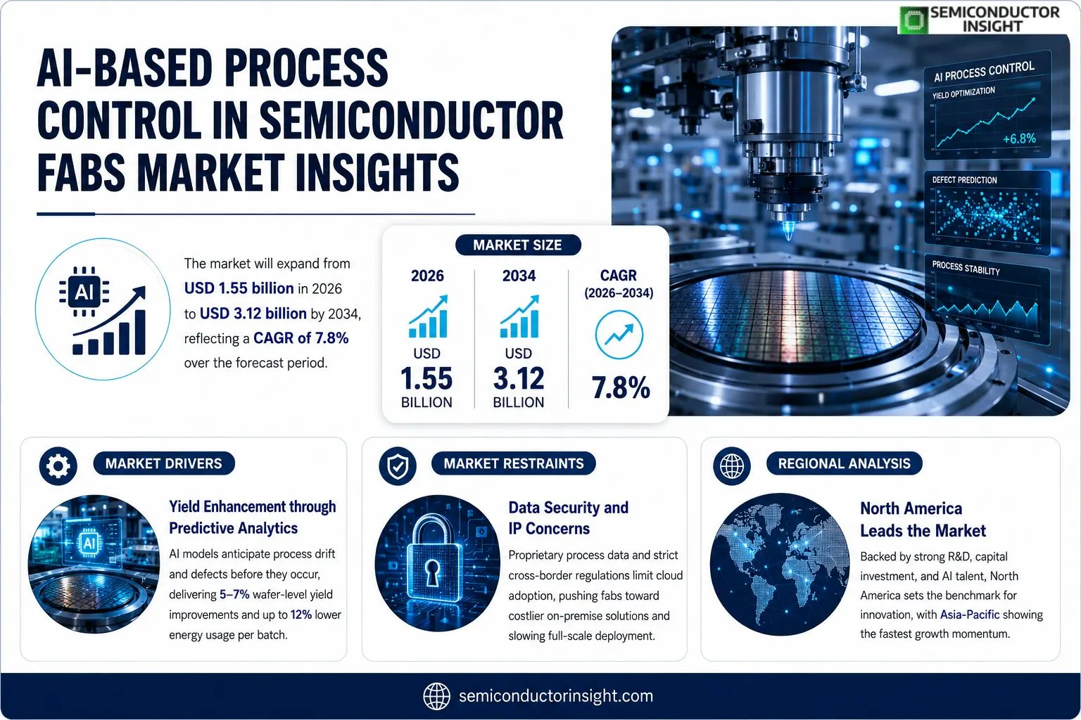
AI‑Based Process Control in Semiconductor Fabs market size was valued at USD 1.45 billion in 2025. The market will expand from USD 1.55 billion in 2026 to USD 3.12 billion by 2034, reflecting a CAGR of 7.8% over the forecast period.
AI‑based process control combines machine‑learning models with high‑frequency sensor streams to continuously adjust deposition, etching, lithography and metrology parameters inside semiconductor fabs. By interpreting patterns that human operators cannot see, the system optimizes cycle time, reduces defect density and improves overall equipment effectiveness across advanced node production.The sector is gaining momentum because manufacturers are seeking higher yields amid escalating design complexity and tighter cost constraints. Capital inflows into next‑generation fab automation, together with rising adoption of predictive analytics platforms such as ASML’s YieldStar AI suite launched in early 2023, are accelerating deployment rates. Moreover, collaborations between equipment suppliers and software specialists are shortening integration cycles, enabling fabs to translate data insights into immediate process adjustments.
MARKET DRIVERS
Yield Enhancement through Predictive Analytics
The integration of machine‑learning models into process control loops enables fabs to anticipate drift before it manifests as defectivity. Recent deployments have shown wafer‑level yield lifts of 5‑7%, a margin that directly improves profitability in a sector where each percentage point is worth millions.
Cost Efficiency from Real‑Time Optimization
By continuously calibrating temperature, pressure, and gas‑flow parameters, AI‑based platforms trim cycle times and reduce consumable waste. Operators report up to 12% lower energy usage per batch, turning what was once a fixed overhead into a variable that can be actively managed.
➤ AI‑driven feedback loops have cut cycle times by as much as 12% in leading 300 mm fabs.
These operational gains sharpen the competitive edge of early adopters, making AI-Based Process Control in Semiconductor Fabs Market a focal point for capital allocation as manufacturers chase incremental margin improvements.
MARKET CHALLENGES
Integration Complexity with Legacy Equipment
Most fabs operate a heterogeneous mix of 1970s‑era process tools that lack native digital interfaces. Retrofitting such assets with AI‑ready sensors often requires custom engineering, inflating project timelines and budgets beyond initial estimates.
Other Challenges
Skill Gap
The scarcity of engineers who combine semiconductor process expertise with deep‑learning proficiency forces companies to outsource talent, driving up labor costs and slowing knowledge transfer to in‑house teams.
MARKET RESTRAINTS
Data Security and IP Concerns
AI models ingest massive volumes of process telemetry, much of which is classified as proprietary. Firms wary of exposing such data to cloud‑based services may limit adoption, opting for on‑premise solutions that carry higher upfront cost.In addition, cross‑border data transfer regulations impose strict controls on where raw sensor data can be stored or processed, adding another layer of compliance overhead that can deter multinational roll‑outs.
MARKET OPPORTUNITIES
Edge‑AI Deployment for On‑Fab Decision Making
Placing inferencing engines at the equipment level eliminates latency associated with centralized cloud analysis. Early pilots indicate a 15% reduction in defect detection time, allowing operators to intervene before a full wafer is compromised.Strategic alliances between semiconductor equipment OEMs and AI software vendors are emerging, offering bundled solutions that accelerate time‑to‑value and reduce integration risk for end users.The convergence of 5G‑enabled factories and increasingly modular AI toolkits creates a fertile environment for niche startups to commercialize specialized models, further diversifying AI-Based Process Control in Semiconductor Fabs Market.
AI-Based Process Control in Semiconductor Fabs Market Trends
Advanced Yield Optimization Through Real‑Time AI Feedback
Manufacturers are increasingly relying on AI‑Based Process Control in Semiconductor Fabs Market solutions that fuse sensor streams with adaptive algorithms. By continuously calibrating lithography exposure, etch chemistry and deposition parameters, these platforms trim variability that historically required manual intervention. The result is a tighter distribution of critical dimensions, which translates into measurable yield lifts across high‑mix production lines. Operators report that the closed‑loop capability shortens the time required to qualify new process windows, allowing faster adoption of advanced nodes without compromising defect density.
Other Trends
Strategic Consolidation Among Tool Suppliers
Leading equipment makers such as Applied Materials, ASML Holding, Siemens Digital Industries Software and KLA Corporation have intensified partnership activity. Recent joint development agreements focus on embedding AI modules directly into process hardware, while selective acquisitions bring specialized data‑analytics teams into established product portfolios. This consolidation reduces integration friction for fabs, delivering a more coherent software stack that can be scaled across multiple tool families.
Edge‑AI Workloads Driving Tighter Process Controls
The surge in edge‑AI accelerator deployment pressures manufacturers to meet stricter power‑efficiency and reliability targets. Since silicon attains its performance envelope through precise control of transistor geometry, any deviation can erode the energy budget of downstream AI chips. AI‑Based Process Control in Semiconductor Fabs Market offerings therefore focus on predictive maintenance and anomaly detection, ensuring that wafer‑level imperfections are caught before they propagate to final products. This proactive stance not only safeguards device performance but also curtails scrap rates that would otherwise inflate production costs.
COMPETITIVE LANDSCAPE
Key Industry Players
AI‑Based Process Control in Semiconductor Fabteries – Competitive Overview
Applied Materials commands the front‑line of AI‑enhanced process control, leveraging its extensive equipment portfolio and the recent collaboration with Nvidia to embed GPU‑accelerated inference directly into lithography and etch tools. This alliance blends deep domain expertise with high‑performance computing, allowing fabs to react to wafer‑level anomalies in near‑real time. Siemens, anchored by its industrial‑automation heritage, partners with IBM to deliver predictive‑maintenance platforms that sit atop legacy fab assets, creating a hybrid ecosystem where legacy and next‑gen lines coexist. The architecture of the market is therefore shaped by a handful of integrators that control both the hardware stack and the AI software layer, raising entry barriers for newcomers and concentrating bargaining power among these few large players.Beyond the headline names, a constellation of specialized firms fuels the ecosystem. Tokyo Electron and ASML contribute cutting‑edge exposure and metrology hardware that feed high‑resolution sensor streams into AI models. KLA Corporation and Lam Research focus on defect detection and deposition control, respectively, embedding machine‑learning kernels within their tool firmware. Chipmakers such as Intel, Samsung Electronics, and TSMC are increasingly internalising algorithm development to tailor control loops for advanced nodes, while startups like AEye and Cognitec provide niche analytics services that augment the broader platform. The diversity of these participants creates a layered supply chain where equipment vendors, software specialists, and fab operators each capture distinct value streams.
List of Key AI-Based Process Control in Semiconductor Fabs Companies Profiled
- Applied Materials
- Nvidia
- Siemens
- IBM
- Tokyo Electron
- ASML
- KLA Corporation
- Lam Research
- Intel
- Samsung Electronics
- TSMC
- Foundries
- AMD
- Cognitec
- AEye
Segment Analysis:
| Segment Category | Sub-Segments | Key Insights |
| By Type |
|
Algorithmic Control
|
| By Application |
|
Lithography Process Control
|
| By End User |
|
Foundries
|
| By Technology Integration |
|
Edge‑AI Embedded Controllers
|
| By Process Step Focus |
|
Yield Prediction and Optimization
|
Regional Analysis: AI-Based Process Control in Semiconductor Fabs Market
North America
Early‑stage fabs are integrating reinforcement‑learning controllers that continuously refine etch parameters, cutting cycle times by a perceptible margin. Collaboration between chip designers and AI specialists yields customized models that translate design intent directly into process recipes, minimizing manual translation errors.
Universities in the Midwest now offer joint degrees in semiconductor engineering and data analytics, feeding a pipeline of professionals who can bridge the cultural gap between process engineers and AI researchers, thereby lowering adoption friction.
The Federal Trade Commission has issued guidance on algorithmic transparency for critical infrastructure, prompting fabs to embed audit trails within their AI control loops, which in turn builds confidence among OEM customers.
AI platforms now communicate directly with upstream material suppliers, forecasting raw‑material consumption based on predicted wafer yields, which reduces inventory buffers and aligns logistics with real‑time production forecasts.
Europe
European fabs benefit from a coordinated policy agenda that ties AI research funding to sustainable manufacturing goals. The emphasis on energy‑efficient process control drives the development of algorithms that balance yield improvements with power consumption constraints. Cross‑border research consortia, particularly in Germany and the Netherlands, enable shared data pools while respecting GDPR mandates, creating a nuanced approach to model training that respects privacy without sacrificing accuracy. OEMs in the region are leveraging this framework to differentiate their high‑volume manufacturing services, positioning themselves as low‑carbon, high‑precision alternatives for automotive and industrial chip customers.
Asia‑Pacific
In Asia‑Pacific, the sheer scale of fab construction projects fuels an appetite for AI‑Based Process Control in Semiconductor Fabs Market solutions that can be rolled out across multiple lines simultaneously. Governments in Taiwan, South Korea, and Singapore are offering tax incentives tied to digital transformation milestones, prompting manufacturers to embed predictive monitoring as a condition for subsidy eligibility. However, talent scarcity in advanced AI disciplines forces many fabs to partner with cloud providers, importing expertise while attempting to retain proprietary process knowledge. The resulting hybrid model accelerates capability gains but introduces new considerations around data sovereignty.
South America
South American chip assembly and testing facilities are beginning to experiment with AI‑driven metrology to improve defect detection in legacy processes. Although the regional market remains modest, early pilots demonstrate that even incremental yield gains can justify the investment given the higher cost of imported equipment. Partnerships with North American technology firms bring best‑practice frameworks, while local universities start to embed semiconductor analytics into engineering curricula, laying groundwork for a future talent pipeline.
Middle East & Africa
The Middle East & Africa region leverages its strategic position in the supply chain to attract semiconductor investments that are keen on diversifying production bases. Emerging AI labs in the United Arab Emirates focus on low‑latency edge control algorithms, catering to fabs that aim to reduce time‑to‑market for specialized chips. Meanwhile, in South Africa, pilot programs are exploring AI‑assisted process optimization for modest volume fabs, highlighting a nascent but growing interest that could evolve as regional policy incentives mature.
Report Scope
This market research report provides a comprehensive analysis of the AI-Based Process Control in Semiconductor Fabs Market , covering the forecast period 2026–2034. It offers detailed insights into market dynamics, technological advancements, competitive landscape, and key trends shaping the industry.
Key focus areas of the report include:
- Market Overview: The report begins with an overview outlining its current market scenario, key growth indicators, and industry transformation drivers. It discusses macroeconomic factors, demand–supply balance, regulatory landscape, and the strategic role of semiconductors in powering advancements across industries such as automotive, telecommunications, consumer electronics, and industrial automation.
- Market Size & Forecast: Historical data and future projections for revenue, unit shipments, and market value across major regions and segments.
- Segmentation Analysis: Detailed breakdown by product type, technology, application, and end-user industry to identify high-growth segments and investment opportunities.
- Regional Insights: Insights into market performance across North America, Europe, Asia-Pacific, Latin America, and the Middle East & Africa, including country-level analysis where relevant.
- Competitive Landscape: Profiles of leading market participants, including their product offerings, R&D focus, manufacturing capacity, pricing strategies, and recent developments such as mergers, acquisitions, and partnerships.
- Technology Trends & Innovation: Assessment of emerging technologies, integration of AI/IoT, semiconductor design trends, fabrication techniques, and evolving industry standards.
- Market Drivers & Restraints: Evaluation of factors driving market growth along with challenges, supply chain constraints, regulatory issues, and market-entry barriers.
- Stakeholder Insights: Insights for component suppliers, OEMs, system integrators, investors, and policymakers regarding the evolving ecosystem and strategic opportunities.
Primary and secondary research methods are employed, including interviews with industry experts, data from verified sources, and real-time market intelligence to ensure the accuracy and reliability of the insights presented.
FREQUENTLY ASKED QUESTIONS:
What is the current market size of AI-Based Process Control in Semiconductor Fabs Market?
-> AI-Based Process Control in Semiconductor Fabs Market was valued at USD 2.48 billion in 2025 and is expected to reach USD 4.79 billion by 2034.
Which key companies operate in AI-Based Process Control in Semiconductor Fabs Market?
-> Key players include Applied Materials, ASML Holding, Siemens Digital Industries Software, and KLA Corporation, among others.
What are the key growth drivers?
-> Key growth drivers include the need for higher throughput, increasing device complexity, edge‑AI workload adoption, and budget pressures driving cost‑effective automation.
Which region dominates the market?
-> The provided data does not specify a dominant region; the market is presented on a basis.
What are the emerging trends?
-> Emerging trends include integration of machine‑learning algorithms with real‑time sensor data, adaptive control of lithography and etch processes, and expanded use of AI‑driven defect detection.

Get Sample Report PDF for Exclusive Insights
Report Sample Includes
- Table of Contents
- List of Tables & Figures
- Charts, Research Methodology, and more...
 Download Sample Report PDF


