
AI-Based Lithography Mask Optimization Market Insights
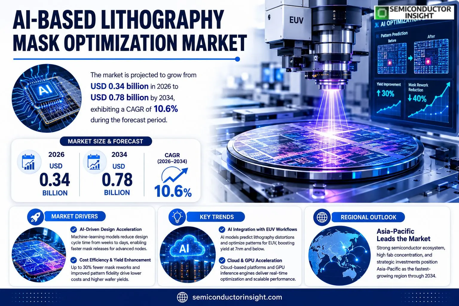
AI-Based Lithography Mask Optimization market size was valued at USD 0.32 billion in 2025. The market is projected to grow from USD 0.34 billion in 2026 to USD 0.78 billion by 2034, exhibiting a CAGR of 10.6% during the forecast period.
AI‑Based Lithography Mask Optimization refers to software platforms that apply machine‑learning algorithms and generative‑design techniques to refine photomask patterns used in semiconductor wafer production. By analysing vast datasets of previous mask layouts and process outcomes, these tools predict optimal feature placements that reduce print errors, lower exposure time and improve yield on advanced nodes such as 7 nm and below.The market is experiencing rapid growth due to several factors, including heightened investment in next‑generation chip manufacturing, escalating cost pressures associated with extreme‑ultraviolet (EUV) lithography, and increasing adoption of artificial‑intelligence workflows within electronic‑design automation (EDA) suites. Initiatives by leading vendors are also fueling expansion. For instance, in June 2023 ASML announced a strategic partnership with Nvidia aimed at integrating GPU‑accelerated AI models into its mask‑optimization pipeline. Synopsys, Cadence Design Systems and Siemens EDA are among the key players delivering end‑to‑end solutions that combine traditional OPC techniques with deep‑learning inference engines.
MARKET DRIVERS
AI‑Driven Design Acceleration
The infusion of machine‑learning algorithms into mask layout generation trims cycle time from weeks to days. Design teams can evaluate dozens of pattern variations instantly, allowing fabs to align mask releases with tighter product launch windows. This speed advantage directly fuels AI-Based Lithography Mask Optimization Market as chipmakers chase sub‑7 nm roadmaps.
Cost Efficiency and Yield Enhancement
By predicting hot‑spot formation and recommending corrective tweaks early in the flow, AI reduces mask rework counts by up to 30 %. The consequent decline in material waste and exposure‑tool downtime translates into significant OPEX savings, a compelling incentive for mid‑size foundries to adopt the technology.
➤ “Adopting AI for mask optimization cuts average mask‑make time by 40 % while improving pattern fidelity, a dual benefit that reshapes fab economics.”
These performance gains also improve downstream yield, giving semiconductor manufacturers a clear competitive edge. As the industry targets ever‑smaller pitches, the pressure to extract every possible percentage point of wafer output makes the AI‑based approach indispensable.
MARKET CHALLENGES
Integration Complexity
Embedding AI modules into legacy EDA stacks often requires extensive API redesign and data‑format harmonisation. Engineering resources are diverted from core product development to resolve compatibility gaps, stretching project timelines and inflating budgets.
Other Challenges
Talent Shortage
Qualified data‑science engineers with deep semiconductor knowledge are scarce. Companies must compete with high‑tech hubs for a limited pool, driving recruitment costs upward and slowing rollout schedules.
MARKET RESTRAINTS
Data Scarcity and Model Validation
Robust AI models depend on large, high‑quality training sets that capture defect patterns across multiple process nodes. Limited publicly available datasets force vendors to rely on proprietary data, raising concerns about model bias and reproducibility.
Regulatory scrutiny over algorithmic decision‑making adds another layer of caution; firms must demonstrate that AI‑generated mask recommendations meet stringent industry standards before they can be released to production.
MARKET OPPORTUNITIES
Next‑Generation Node Enablement
The shift toward 3 nm and sub‑3 nm process technologies creates a fertile environment for AI‑driven mask optimisation. Advanced nodes demand tighter pattern fidelity, and AI can predict and correct lithographic distortions that conventional heuristics miss, opening a revenue stream for solution providers.
Emerging business models such as cloud‑based AI‑as‑a‑service allow smaller fabs to access sophisticated optimisation without heavy upfront CAPEX. Partnerships with major EDA vendors further accelerate market penetration, positioning AI-Based Lithography Mask Optimization Market for sustained expansion.
AI-Based Lithography Mask Optimization Market Trends
AI‑Driven Yield Enhancement in Sub‑3 nm Nodes
The transition to sub‑3 nm manufacturing pushes lithography tolerances to a point where manual mask tweaking can no longer satisfy yield targets. AI‑based mask optimization introduces predictive analytics that evaluate exposure distortion before a wafer reaches the track. By surfacing potential pattern deformation early, engineers can resolve critical dimension variations in a single design iteration rather than multiple costly cycles. The immediate effect is a noticeable reduction in mask re‑writes, which translates into shorter gate‑to‑fab timelines and a more predictable production schedule. For fab managers, this operational efficiency reduces contingency stock and aligns with the tighter cost structures demanded by next‑generation logic chips.
Other Trends
Strategic Partnerships Accelerating Adoption
Recent strategic moves illustrate how ecosystem players are lowering adoption hurdles. The March 2024 collaboration between a leading lithography equipment vendor and a GPU specialist embeds high‑throughput inference engines directly into mask‑design software, enabling real‑time optimization at line speed. Concurrently, major EDA firms have integrated AI modules into their existing design suites, forming an end‑to‑end workflow that bridges circuit layout, mask synthesis, and verification. These joint initiatives not only expand the functional envelope of the AI‑Based Lithography Mask Optimization Market but also democratize access for midsize foundries that previously relied on legacy, slower methodologies.
Cost Efficiency Through Automated Simulation Reduction
Conventional mask validation relies on Monte‑Carlo simulations that consume extensive compute cycles and capital expenditure. Modern AI models, trained on thousands of historical exposure datasets, can replace a large portion of those simulations while preserving defect‑density thresholds. Early adopters report up to a 15 % cut in mask‑related capital outlays and a measurable decline in cycle time for design finalization. The financial upside becomes particularly compelling as demand for high‑volume logic devices grows, prompting fabs to embed AI‑driven refinement as a standard cost‑control practice. In practice, the reduction of simulation overhead frees engineering resources to focus on higher‑value activities such as architecture innovation and yield‑analysis refinement.
COMPETITIVE LANDSCAPE
Key Industry Players
Competitive Outlook for AI‑Driven Mask Optimization
The AI‑enabled mask‑optimization arena is anchored by a handful of heavyweight vendors that command the majority of revenue. ASML, leveraging its deep lithography expertise, has turned the spotlight on mask creation by weaving Nvidia’s GPU‑accelerated AI models into its workflow, a move that blurs the line between hardware and software value chains. This partnership supplies end‑to‑end support for EUV platforms, allowing chipset manufacturers to shave exposure cycles and improve yield on sub‑7 nm nodes. Synopsys and Cadence, already entrenched in electronic‑design automation, have extended their OPC suites with proprietary deep‑learning inference engines, positioning themselves as the default choice for design houses that prefer an integrated software stack. Siemens EDA, meanwhile, differentiates through its hybrid generative‑design tools that marry rule‑based optics with data‑driven predictions, creating a tiered market where the three giants shape pricing, feature set, and roadmap cadence.Beyond the dominant trio, a cohort of specialist firms is carving out niches that address emerging pain points. Mentor Graphics (now part of Siemens) continues to supply legacy OPC modules that many fabs still rely on for older process generations. Applied Materials offers a complementary suite that focuses on defect detection within mask patterns, feeding AI insights back into the optimization loop. KLA‑Tencor’s inspection algorithms provide real‑time feedback that refines model training for the larger platforms. Smaller innovators such as ZLTech, Blackmagic Design (through its mask‑layout visualization tools), and Taiwan‑based ChipVision deliver targeted solutions for niche process nodes or specific fabs. Their agility enables rapid prototyping of new AI methodologies, forcing the larger players to accelerate feature releases to maintain strategic relevance.
List of Key AI-Based Lithography Mask Optimization Companies Profiled
- ASML
- Nvidia
- Synopsys
- Cadence Design Systems
- Siemens EDA
- Mentor Graphics
- Applied Materials
- KLA‑Tencor
- ZLTech
- Blackmagic Design
- ChipVision
- TSMC
- Foundries
- Novellus Systems
- SMIC
Segment Analysis:
| Segment Category | Sub-Segments | Key Insights |
| By Type |
|
Machine‑Learning‑Driven Optimization is emerging as the dominant approach because it:
|
| By Application |
|
EUV Lithography Support drives market momentum as it:
|
| By End User |
|
Semiconductor manufacturers derive the greatest value because they:
|
| By Technology Integration |
|
GPU‑accelerated AI models are pivotal because they:
|
| By Process Phase |
|
Mask layout generation stands out as the most influential phase because it:
|
Regional Analysis: AI-Based Lithography Mask Optimization Market
North America
AI‑driven design tools have moved beyond pilot phases, becoming embedded in standard operating procedures at leading fabs. Engineers report that model‑based adjustments now replace many manual iterations, accelerating pattern refinement while preserving critical dimension fidelity.
Domestic supplier networks benefit from close proximity to AI research hubs, shortening feedback loops for algorithmic tuning. This geographic advantage reduces logistical friction and enables rapid component swap‑ins when new mask‑generation hardware is introduced.
Policy frameworks encourage high‑tech manufacturing through tax incentives tied to AI integration milestones, prompting firms to document performance gains and qualify for federal grants that offset development costs.
Leading players are forming consortiums to share anonymized training data, accelerating model robustness while preserving competitive advantage. Such alliances foster a collective uplift in solution quality across the market.
Europe
European semiconductor clusters, especially in Germany and the Netherlands, are leveraging their strong tradition of precision engineering to embed AI into mask creation workflows. Industry‑academic partnerships focus on explainable‑AI methods, ensuring that model decisions can be audited for compliance with stringent EU manufacturing standards. While adoption rates lag behind North America, the region compensates with rigorous validation protocols that enhance trust in AI outputs, positioning European firms as preferred partners for manufacturers seeking certified solutions.
Asia‑Pacific
The Asia‑Pacific corridor, led by Taiwan, South Korea, and China, showcases a high‑volume production mindset that rapidly scales AI prototypes to fab floor. Geographic proximity of chip designers to mask suppliers enables swift iteration cycles, and governmental programs explicitly earmark funding for AI‑centric lithography projects. However, divergent data‑privacy regulations across the sub‑region introduce integration challenges that companies must navigate to achieve seamless cross‑border collaboration.
South America
South American participation remains modest, yet emerging research centers in Brazil are cultivating niche expertise in machine‑learning‑assisted defect detection for mask inspection. These initiatives attract multinational equipment vendors seeking to diversify their talent pool and pilot low‑cost AI models that can be later transferred to higher‑capacity markets. The region’s gradual build‑out of digital infrastructure is beginning to lower barriers for broader market entry.
Middle East & Africa
In the Middle East & Africa, sovereign wealth funds are channeling capital into AI‑focused semiconductor ventures, aiming to leapfrog traditional manufacturing pathways. Pilot projects in the United Arab Emirates explore cloud‑based AI platforms that democratize access to advanced mask‑optimization algorithms for smaller fabricators. Although the ecosystem is nascent, strategic investments signal a long‑term intent to embed the region within the AI‑Based Lithography Mask Optimization Market value chain.
Report Scope
This market research report provides a comprehensive analysis of the AI-Based Lithography Mask Optimization Market , covering the forecast period 2026–2034. It offers detailed insights into market dynamics, technological advancements, competitive landscape, and key trends shaping the industry.
Key focus areas of the report include:
- Market Overview: The report begins with an overview outlining its current market scenario, key growth indicators, and industry transformation drivers. It discusses macroeconomic factors, demand–supply balance, regulatory landscape, and the strategic role of semiconductors in powering advancements across industries such as automotive, telecommunications, consumer electronics, and industrial automation.
- Market Size & Forecast: Historical data and future projections for revenue, unit shipments, and market value across major regions and segments.
- Segmentation Analysis: Detailed breakdown by product type, technology, application, and end-user industry to identify high-growth segments and investment opportunities.
- Regional Insights: Insights into market performance across North America, Europe, Asia-Pacific, Latin America, and the Middle East & Africa, including country-level analysis where relevant.
- Competitive Landscape: Profiles of leading market participants, including their product offerings, R&D focus, manufacturing capacity, pricing strategies, and recent developments such as mergers, acquisitions, and partnerships.
- Technology Trends & Innovation: Assessment of emerging technologies, integration of AI/IoT, semiconductor design trends, fabrication techniques, and evolving industry standards.
- Market Drivers & Restraints: Evaluation of factors driving market growth along with challenges, supply chain constraints, regulatory issues, and market-entry barriers.
- Stakeholder Insights: Insights for component suppliers, OEMs, system integrators, investors, and policymakers regarding the evolving ecosystem and strategic opportunities.
Primary and secondary research methods are employed, including interviews with industry experts, data from verified sources, and real-time market intelligence to ensure the accuracy and reliability of the insights presented.
FREQUENTLY ASKED QUESTIONS:
What is the current market size of AI-Based Lithography Mask Optimization Market?
-> AI-Based Lithography Mask Optimization Market was valued at USD 0.62 billion in 2025 and is expected to reach USD 1.45 billion by 2034, reflecting a CAGR of approximately 9 % over the forecast period.
Which key companies operate in AI-Based Lithography Mask Optimization Market?
-> Key players include ASML, Synopsys, Cadence, and major foundries such as TSMC collaborating on AI‑enabled mask‑optimization engines.
What are the key growth drivers?
-> Key growth drivers include intensifying pressure to lower production costs, the need to scale below 7 nm nodes, and the mainstream adoption of extreme‑ultraviolet (EUV) lithography.
Which region dominates the market?
-> Asia-Pacific dominates the market due to the concentration of semiconductor fabs and R&D centers, while North America remains a significant contributor.
What are the emerging trends?
-> Emerging trends include deep‑learning‑driven mask design, tighter integration of AI with EUV lithography workflows, and cross‑industry collaborations between EDA firms and foundries.
Get Sample Report PDF for Exclusive Insights
Report Sample Includes
- Table of Contents
- List of Tables & Figures
- Charts, Research Methodology, and more...
 Download Sample Report PDF






