
AI-Based Backside Chipping Inspection After Dicing Market Insights
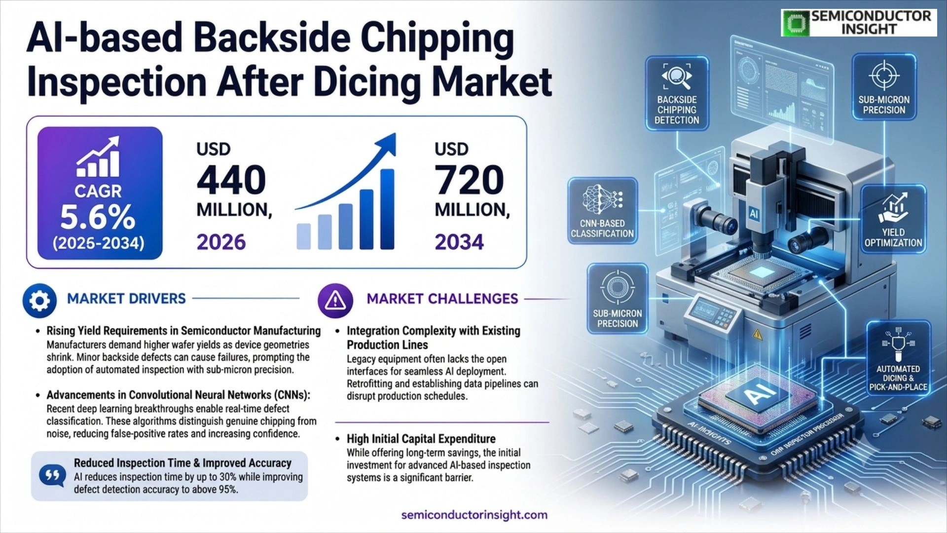
Global AI-based backside chipping inspection after dicing market size was valued at USD 420 million in 2025. The market is projected to grow from USD 440 million in 2026 to USD 720 million by 2034, exhibiting a CAGR of 5.6% during the forecast period.
This technology combines high‑resolution optical imaging with deep‑learning algorithms to identify microscopic chips, cracks or contamination on the wafer backside immediately after dicing. By automating defect detection, it reduces manual review time and enhances overall yield for advanced semiconductor manufacturing.
The market is accelerating because semiconductor fabs are pushing toward sub‑7 nm nodes, where even minor backside defects can cause costly failures. Moreover, rising adoption of Industry 4.0 practices and the availability of edge‑AI processors are driving investment. Leading suppliers such as KLA Corporation, Applied Materials, ASML Holding and Advantest are expanding their portfolios with AI‑enhanced inspection modules to meet growing demand.
MARKET DRIVERS
Rising Yield Requirements in Semiconductor Manufacturing
AI-based backside chipping Inspection After Dicing Market is propelled by manufacturers’ demand for higher wafer yields. As device geometries shrink, even minor backside defects can cause catastrophic failures, prompting fabs to adopt automated inspection systems that detect chipping with sub‑micron precision.
Advancements in Convolutional Neural Networks
Recent breakthroughs in deep learning,particularly in convolutional neural networks (CNNs),enable real‑time defect classification. These algorithms can distinguish genuine chipping from noise, reducing false‑positive rates and increasing operator confidence.
➤ AI reduces inspection time by up to 30 % while improving defect detection accuracy to above 95 %.
Combined, higher yield pressures and sophisticated AI models create a compelling value proposition that accelerates adoption across both mature and cutting‑edge fabs.
MARKET CHALLENGES
Integration Complexity with Existing Production Lines
Legacy equipment often lacks the open interfaces required for seamless AI deployment. Retrofitting sensors and establishing data pipelines can disrupt production schedules, leading firms to postpone full‑scale rollouts.
Other Challenges
Data Labeling and Model Training
Accurate training sets demand painstaking manual annotation of backside images, which is both time‑consuming and costly. Insufficient labeled data hampers model robustness, especially for low‑volume specialty wafers.
Moreover, the need for continuous model updates to accommodate new device architectures adds operational overhead, challenging smaller fabs with limited engineering resources.
MARKET RESTRAINTS
High Initial Capital Expenditure
Deploying AI‑driven inspection stations involves substantial upfront costs for high‑resolution cameras, lighting arrays, and compute infrastructure. For many mid‑size manufacturers, the payback horizon extends beyond typical capital‑budget cycles, restraining market penetration.
In addition, compliance with stringent clean‑room standards often necessitates custom‑engineered hardware enclosures, further inflating project budgets.
MARKET OPPORTUNITIES
Emerging Applications in Advanced Packaging
The shift toward heterogeneous integration and 3D‑IC packaging creates new inspection demands. AI‑based backside chipping detection can be adapted to verify micro‑bump integrity and under‑fill quality, unlocking revenue streams beyond traditional wafer dicing.
Geographically, manufacturers in East Asia are accelerating investments in smart fab initiatives, presenting a fertile market for vendors that can offer turn‑key AI solutions tailored to regional compliance frameworks.
AI-Based Backside Chipping Inspection After Dicing Market Trends
Increasing Adoption of Edge‑AI for Real‑Time Defect Detection
The semiconductor industry is witnessing a rapid shift toward edge‑AI processors that can run deep‑learning models directly on inspection equipment. By embedding inference engines at the front end of the production line, manufacturers achieve sub‑second detection of backside chips and cracks immediately after dicing. This capability reduces reliance on off‑site data centers, lowers latency, and curtails the total cost of ownership. Early adopters report yield improvements of 2‑3 % because defective wafers are removed before subsequent processing steps, which in turn protects downstream equipment from premature wear.
Other Trends
Integration with Industry 4.0 Data Platforms
Inspection systems are increasingly being linked to cloud‑based analytics hubs that aggregate defect data across multiple fabs. The unified view enables cross‑facility benchmarking and supports predictive maintenance of dicing saws and handling robots. As a result, operators can anticipate process drift before it translates into yield loss. The trend aligns with broader Industry 4.0 initiatives that emphasize data‑driven decision making and seamless machine‑to‑machine communication.
Expansion of AI‑Enhanced Inspection Modules by Established Equipment Vendors
Major suppliers such as KLA Corporation, Applied Materials, ASML Holding and Advantest have introduced next‑generation inspection modules that embed convolutional neural networks within their optical platforms. These modules offer higher resolution imaging combined with automated defect classification, allowing technicians to focus on root‑cause analysis rather than manual review. The product roadmap of these vendors shows a clear emphasis on modular AI add‑ons, which can be retrofitted to existing equipment, thereby extending the lifecycle of capital assets.
COMPETITIVE LANDSCAPE
Key Industry Players
AI-Based Backside Chipping Inspection After Dicing Market Competitive Overview
The market is predominantly led by integrated instrumentation giants such as KLA Corporation, Applied Materials, ASML Holding, and Advantest. These firms leverage deep‑learning‑enabled optical sensors and edge‑AI processors to offer turnkey inspection modules that are tightly coupled with dicing equipment. Their extensive global service networks, strong R&D pipelines, and strategic acquisitions have created a tier‑one tiered structure where the bulk of high‑volume fab contracts are awarded to these incumbents, reinforcing a consolidated supply chain for sub‑7 nm node production.
Beyond the core tier, a diverse set of niche innovators is expanding the competitive set. Tokyo Electron, Hitachi High‑Technologies, and Nanometrics provide specialized high‑resolution imaging and metrology solutions that complement the primary vendors. Camtek, ULVAC, MKS Instruments, SÜSS MicroTec, H&K Group, Sentech, and OMM focus on vertical integration, customized AI algorithms, or complementary wafer‑handling equipment, enabling fabs to address specific defect‑signature challenges and to diversify risk across multiple suppliers.
List of Key AI-Based Backside Chipping Inspection After Dicing Companies Profiled
- KLA Corporation
- Applied Materials
- ASML Holding
- Advantest
- Tokyo Electron
- Hitachi High‑Technologies
- Nanometrics
- Camtek
- ULVAC
- MKS Instruments
- SÜSS MicroTec
- H&K Group
- Sentech
- OMM
Segment Analysis:
| Segment Category | Sub-Segments | Key Insights |
| By Type |
|
Optical Imaging Systems are rapidly becoming the core enabler for reliable backside defect detection. They provide high‑resolution visual capture that feeds directly into AI models, ensuring that subtle chips are not missed.
|
| By Application |
|
Yield Optimization drives strategic adoption of AI‑based inspection because it directly influences wafer profitability. The insight loop links backside defect data to process adjustments, creating a proactive quality culture.
|
| By End User |
|
Foundry Service Providers are emerging as the leading end‑user segment, leveraging AI inspection to meet diverse customer specifications across multiple process nodes.
|
| By Inspection Modality |
|
Real‑Time Edge AI is gaining traction because it processes inspection data directly on the production line, eliminating latency and ensuring immediate corrective action.
|
| By Value‑Chain Stage |
|
Post‑Dicing Inspection is the focal point for AI‑driven backside defect detection, as it captures the exact moment chips may form and informs subsequent handling steps.
|
Regional Analysis: AI-Based Backside Chipping Inspection After Dicing
North America
The North American segment accounts for the largest installed base of AI inspection tools, with compound annual growth projected to outpace global averages as manufacturers scale to 300 mm and beyond.
Drivers include the push for higher yield, increasing adoption of AI‑enabled defect classification, and cost pressures that favor automation over manual inspection.
Standards such as JEDEC and ISO‑26262 influence inspection requirements, prompting firms to embed compliance checks within AI workflows.
Established OEMs are joined by agile startups that specialize in deep‑learning inference, creating a dynamic ecosystem of partnership and competition.
Europe
European semiconductor hubs, particularly in Germany and the Netherlands, are accelerating AI‑Based Backside Chipping Inspection After Dicing adoption through public‑private research consortia. Emphasis on sustainability has prompted manufacturers to seek inspection solutions that minimize waste, while EU funding programs support cross‑border AI projects. Market participants are differentiating by offering modular systems that integrate seamlessly with existing fab lines, allowing incremental upgrades without major capital outlays.
Asia‑Pacific
The Asia‑Pacific region shows rapid expansion as fabs in Taiwan, South Korea, and China scale capacity. Cost‑sensitive players are adopting AI inspection to reduce reliance on expensive manual labor. Local vendors are tailoring algorithms to regional process variations, and strategic partnerships with cloud providers enable scalable data processing. Although regulatory guidance is less prescriptive, industry standards are gradually converging, fostering broader adoption.
South America
South American chip fabrication remains nascent, but early pilots of AI‑Based Backside Chipping Inspection After Dicing are emerging in Brazil’s emerging semiconductor clusters. Companies focus on pilot projects that demonstrate yield improvements, leveraging partnerships with North American technology providers. Market growth is closely tied to government incentives aimed at building a localized semiconductor ecosystem.
Middle East & Africa
Investment in semiconductor manufacturing infrastructure is modest, yet the Middle East & Africa region is positioning itself as a testing ground for AI‑driven inspection services. Pilot deployments in United Arab Emirates tech parks focus on high‑value specialty wafers, using AI to compensate for limited skilled inspection personnel. Growth prospects depend on attracting multinational fab operators and expanding technical talent pools.
Report Scope
This market research report provides a comprehensive analysis of the AI-Based Backside Chipping Inspection After Dicing Market , covering the forecast period 2026–2034. It offers detailed insights into market dynamics, technological advancements, competitive landscape, and key trends shaping the industry.
Key focus areas of the report include:
- Market Overview: The report begins with an overview outlining its current market scenario, key growth indicators, and industry transformation drivers. It discusses macroeconomic factors, demand–supply balance, regulatory landscape, and the strategic role of semiconductors in powering advancements across industries such as automotive, telecommunications, consumer electronics, and industrial automation.
- Market Size & Forecast: Historical data and future projections for revenue, unit shipments, and market value across major regions and segments.
- Segmentation Analysis: Detailed breakdown by product type, technology, application, and end-user industry to identify high-growth segments and investment opportunities.
- Regional Insights: Insights into market performance across North America, Europe, Asia-Pacific, Latin America, and the Middle East & Africa, including country-level analysis where relevant.
- Competitive Landscape: Profiles of leading market participants, including their product offerings, R&D focus, manufacturing capacity, pricing strategies, and recent developments such as mergers, acquisitions, and partnerships.
- Technology Trends & Innovation: Assessment of emerging technologies, integration of AI/IoT, semiconductor design trends, fabrication techniques, and evolving industry standards.
- Market Drivers & Restraints: Evaluation of factors driving market growth along with challenges, supply chain constraints, regulatory issues, and market-entry barriers.
- Stakeholder Insights: Insights for component suppliers, OEMs, system integrators, investors, and policymakers regarding the evolving ecosystem and strategic opportunities.
Primary and secondary research methods are employed, including interviews with industry experts, data from verified sources, and real-time market intelligence to ensure the accuracy and reliability of the insights presented.
FREQUENTLY ASKED QUESTIONS:
What is the current market size of AI-Based Backside Chipping Inspection After Dicing Market?
-> AI-based backside chipping inspection after dicing market is projected to grow from USD 440 million in 2026 to USD 720 million by 2034, exhibiting a CAGR of 5.6% .
Which key companies operate in AI-Based Backside Chipping Inspection After Dicing Market?
-> Key players include KLA Corporation, Applied Materials, ASML Holding, and Advantest, among others.
What are the key growth drivers?
-> Key growth drivers include advancement toward sub‑7 nm nodes, Industry 4.0 adoption, and the availability of edge‑AI processors enabling higher yield and defect detection efficiency.
Which region dominates the market?
-> Asia-Pacific is the fastest‑growing region, while North America holds the largest market share.
What are the emerging trends?
-> Emerging trends include AI‑enhanced inspection modules, integration of deep‑learning algorithms with high‑resolution optical imaging, and edge‑AI processing for real‑time defect detection.

Get Sample Report PDF for Exclusive Insights
Report Sample Includes
- Table of Contents
- List of Tables & Figures
- Charts, Research Methodology, and more...
 Download Sample Report PDF





