X-ray CMOS Image Sensor Market Insights
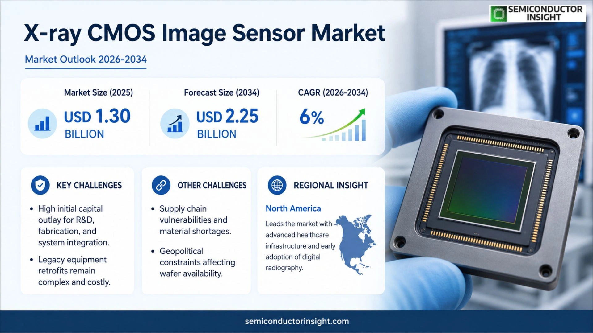
X-ray CMOS Image Sensor market size stood at USD 1.30 billion in 2025 and is set to rise to roughly USD 2.25 billion by 2034, implying a compound annual growth rate of approximately 6 percent over the forecast horizon.
An X-ray CMOS Image Sensor is a semiconductor device that converts X‑ray photons into digital signals for high‑resolution, low‑noise imaging. It finds application across medical diagnostics, industrial inspection, security screening and scientific research, progressively supplanting traditional amorphous‑silicon and CCD detectors. Two detection architectures dominate: indirect conversion,where X‑rays excite a scintillator that emits visible light captured by a CMOS photodiode,and direct conversion,where incident photons generate electron‑hole pairs directly within the semiconductor substrate.
MARKET DRIVERS
Advancements in Sensor Architecture
The shift from traditional charge‑coupled devices to CMOS platforms has unlocked faster readout rates and lower power consumption. Manufacturers are capitalising on these advantages to deliver compact X‑ray systems that fit into modern clinical workflows, thereby encouraging broader adoption across hospitals and imaging centres.
Regulatory Emphasis on Patient Dose Reduction
Health authorities worldwide have tightened exposure limits for diagnostic radiology. CMOS sensors, with their higher quantum efficiency, enable clear images at reduced radiation levels. This compliance pressure nudges equipment suppliers toward integrating CMOS technology, reinforcing market momentum.
➤ “Clinicians report a 30 % drop in average dose when migrating from CCD to CMOS‑based X‑ray units, without compromising diagnostic confidence.”
Beyond clinical settings, emerging sectors such as industrial non‑destructive testing and security screening are recognising the reliability and speed of CMOS detectors. Strategic investments in these verticals are expanding the addressable base for the X‑ray CMOS Image Sensor Market.
MARKET CHALLENGES
High Initial Capital Outlay
Deploying state‑of‑the‑art CMOS modules entails substantial upfront spend on R&D, wafer fabrication, and system integration. Smaller imaging providers often struggle to justify the expense, slowing penetration in cost‑sensitive regions.
Other Challenges
Supply Chain Vulnerabilities
The semiconductor ecosystem faces periodic material shortages and geopolitical constraints, which can disrupt the steady flow of high‑purity silicon wafers required for X‑ray sensor production. Companies must therefore build buffer inventories or diversify sourcing strategies.
Furthermore, legacy equipment fleets dominate many markets, and the retrofit path for older X‑ray cabinets to accept CMOS sensors remains technically intricate, creating a friction point for rapid upgrade cycles.
MARKET RESTRAINTS
Complex Calibration Requirements
CMOS sensors demand precise calibration of gain, offset, and dark current to maintain image uniformity across varying exposure conditions. The need for specialised calibration software and skilled technicians adds operational overhead for end‑users, deterring some potential adopters.
In addition, the relatively short product life cycle of semiconductor components can lead to obsolescence concerns, prompting buyers to favour more established, albeit less efficient, detector technologies.
MARKET OPPORTUNITIES
Integration with AI‑Driven Imaging Workflows
CMOS sensors produce high‑resolution frames at rates that align well with real‑time AI algorithms for anomaly detection and dose optimisation. Vendors that bundle sensor hardware with intelligent software suites can capture premium market share and open recurring‑revenue streams.
Expansion into Portable Diagnostics
The lightweight nature of CMOS devices fuels the development of handheld X‑ray scanners for field hospitals, disaster relief, and veterinary use. This mobility trend creates a niche where traditional bulky detectors cannot compete.
Finally, collaborative R&D programmes between semiconductor foundries and medical‑device OEMs are accelerating the rollout of next‑generation sensors with built‑in radiation‑hardening features, laying the groundwork for broader acceptance in high‑dose industrial environments.
X-ray CMOS Image Sensor Market Trends
Shift Toward Direct‑Conversion Architecture
In 2025 the sector produced roughly 309 million units, with an average unit price of US$ 4.6. The direct‑conversion design, which captures X‑ray photons directly as electron‑hole pairs, is increasingly favored because it eliminates the scintillator layer that adds noise and limits spatial resolution. As manufacturers integrate pixel‑level amplification and faster read‑out circuits, the resulting sensors deliver clearer images with lower exposure times, a benefit that resonates strongly with medical imaging facilities seeking dose‑reduction protocols. The transition also aligns with the broader industry push for compact detector modules that can be embedded in portable C‑arm systems. Consequently, product lines that historically relied on indirect conversion are being re‑engineered, prompting a noticeable realignment of R&D budgets toward semiconductor process optimization and advanced pixel architectures.
Other Trends
Vertical Integration Across the Supply Chain
X-ray CMOS Image Sensor Market exhibits a pronounced vertical hierarchy. Upstream suppliers of high‑purity silicon, lithography equipment, and proprietary IP remain tightly clustered among a few global players, creating a barrier to entry for newcomers. Midstream activities split between integrated device manufacturers (IDM) that own wafer fabs and fabless designers that partner with foundries and OSAT firms. This dual‑model environment has spurred strategic alliances; several leading IDM firms have secured long‑term wafer‑supply contracts while fabless companies leverage the latest 65 nm and 28 nm processes to shrink pixel pitch. Downstream, equipment integrators and system vendors incorporate the sensors into platforms ranging from industrial X‑ray scanners to security portals, reinforcing a feedback loop where application‑driven specifications dictate upstream material and process choices.
Emerging Applications in Industrial Inspection
Industrial inspection represents the fastest‑growing demand segment for X‑ray CMOS sensors. Manufacturers of automotive components, aerospace assemblies, and printed‑circuit boards are adopting high‑dynamic‑range detectors to capture both dense and lightweight features within a single exposure. The ability to operate in global‑shutter mode enables precise motion‑blur elimination, a critical factor for in‑line quality control where production speeds exceed 500 mm/s. As these sectors prioritize yield and defect‑reduction, sensor vendors are introducing hybrid‑APS and sCMOS architectures that combine low‑noise performance with robust data throughput. The resulting ecosystem encourages equipment makers to embed advanced analytics, turning raw image data into actionable process insights. This shift not only expands the addressable market size but also establishes a durable revenue stream for firms that can synchronize sensor capabilities with evolving industrial standards.
COMPETITIVE LANDSCAPE
Key Industry Players
X‑ray CMOS Image Sensor Market – Competitive Overview
Hamamatsu Photonics continues to anchor the high‑resolution segment of the X‑ray CMOS market, leveraging its legacy in photon‑counting detector technology to secure a dominant share of medical‑imaging contracts. Its vertically integrated model,covering crystal growth, sensor design, wafer fabrication and final module assembly,creates a barrier for newcomers and ensures tight control over performance specifications. The firm’s recent rollout of a direct‑conversion sensor line, featuring sub‑5 µm pixel pitches, has compelled OEMs to prioritize a single‑source supply strategy, reinforcing Hamamatsu’s bargaining position across the value chain.
Beyond the tier‑one incumbents, a cluster of specialized firms is reshaping niche applications such as industrial non‑destructive testing, security scanning, and scientific instrumentation. Companies like Teledyne e2v and Tower Semiconductor exploit fab‑less design coupled with advanced foundry partnerships to introduce hybrid‑APS architectures that balance sensitivity and read‑out speed. Meanwhile, Sony Semiconductor Solutions, ON Semiconductor, and STMicroelectronics are translating their consumer‑CIS expertise into ruggedized X‑ray sensors for automotive and logistics sectors. Emerging players,including Gpixel, Canon Electronics, Samsung Electronics, Toshiba, and Fujifilm,are expanding their portfolios through strategic acquisitions or joint ventures, targeting segments where indirect‑conversion designs remain cost‑effective. This diversification of business models enriches the competitive fabric and drives incremental innovation across detection principles.
List of Key X-ray CMOS Image Sensor Companies Profiled
- Hamamatsu Photonics
- Teledyne e2v
- Tower Semiconductor
- Sony Semiconductor Solutions
- ON Semiconductor
- STMicroelectronics
- Gpixel
- Canon Electronics
- Samsung Electronics
- Toshiba
- Fujifilm
- Pixel Sensor Microsystems
Segment Analysis:
| Segment Category | Sub-Segments | Key Insights |
| By Type |
|
Area Sensors are increasingly preferred because they enable high‑resolution imaging across broader fields of view, supporting diverse medical and scientific use cases.
|
| By Application |
|
Medical Imaging drives much of the innovation in X‑ray CMOS sensors, prompting manufacturers to focus on diagnostic quality and workflow efficiency.
|
| By End User |
|
Hospitals & Clinics represent the most mature adoption environment, emphasizing reliability and regulatory compliance.
|
| By Detection Principle |
|
Direct Conversion is gaining prominence due to its ability to simplify the imaging stack and enhance spatial resolution.
|
| By Architecture |
|
Monolithic APS is seen as the architecture of choice for next‑generation X‑ray sensors, enabling tighter process integration.
|
Regional Analysis: X-ray CMOS Image Sensor Market
North America
Clinical imaging centers prioritize CMOS chips for their superior quantum efficiency, which translates into clearer chest radiographs at lower dose levels, a key driver for patient‑centred care pathways.
The FDA’s clear guidance on digital detector performance accelerates market entry for new X‑ray CMOS products, reducing time‑to‑market for innovators.
Proximity to semiconductor foundries allows rapid prototyping and scalability, insulating manufacturers from the volatility that affects overseas production hubs.
Capital‑intensive health systems allocate budgets toward modular CMOS arrays that can be upgraded without replacing entire imaging suites, extending asset life cycles.
Europe
European medical institutions, especially in Germany and France, are integrating X‑ray CMOS sensors to comply with stricter radiation‑exposure limits mandated by EU directives. The emphasis on patient safety drives procurement of detectors that deliver high contrast at reduced dose, prompting vendors to tailor sensor architectures for specific clinical protocols. In parallel, aerospace security agencies are experimenting with CMOS‑based backscatter scanners for cargo inspection, leveraging the technology’s ability to produce real‑time imagery under challenging environmental conditions. Collaborative research programs across the continent, funded by Horizon Europe, focus on hybrid sensor designs that embed AI inference at the pixel level, a move that could reshape workflow efficiencies in radiology departments.
Asia‑Pacific
Rapid urbanization and expanding middle‑class populations in China, India, and Southeast Asia have spurred investment in modern diagnostic facilities. Hospital chains view X‑ray CMOS sensors as a means to differentiate service offerings, emphasizing faster patient turnover and lower operational costs. Government incentives for digital health transformation further lower entry barriers for domestic manufacturers, many of which are establishing joint ventures with established Western firms to acquire process know‑how. The region also witnesses growing demand from industrial nondestructive testing, where high‑speed CMOS cameras enable real‑time flaw detection on production lines, supporting the broader manufacturing upgrade agenda.
South America
In Brazil and Chile, public‑private partnerships are accelerating the rollout of digital radiography platforms equipped with CMOS sensors, driven by national health strategies aimed at reducing diagnostic backlogs. Budget constraints encourage hospitals to select modular detector systems that can be retrofitted into existing X‑ray cabinets, extending the utility of legacy equipment. Moreover, the mining sector leverages X‑ray CMOS imaging for on‑site material analysis, valuing the sensor’s robustness and capacity to operate under harsh field conditions without compromising image fidelity.
Middle East & Africa
The Gulf Cooperation Council states invest heavily in state‑of‑the‑art medical campuses, where X‑ray CMOS technology aligns with aspirations for precision diagnostics and patient‑centric care models. Meanwhile, emerging markets in Sub‑Saharan Africa prioritize cost‑effective imaging solutions; CMOS sensors, with their lower power consumption and simplified cooling requirements, fit these constraints. International NGOs support capacity‑building initiatives that introduce digital X‑ray systems to rural clinics, positioning CMOS platforms as a bridge between limited resources and modern diagnostic capabilities.
Report Scope
This market research report provides a comprehensive analysis of the X-ray CMOS Image Sensor Market , covering the forecast period 2026–2034. It offers detailed insights into market dynamics, technological advancements, competitive landscape, and key trends shaping the industry.
Key focus areas of the report include:
- Market Overview: The report begins with an overview outlining its current market scenario, key growth indicators, and industry transformation drivers. It discusses macroeconomic factors, demand–supply balance, regulatory landscape, and the strategic role of semiconductors in powering advancements across industries such as automotive, telecommunications, consumer electronics, and industrial automation.
- Market Size & Forecast: Historical data and future projections for revenue, unit shipments, and market value across major regions and segments.
- Segmentation Analysis: Detailed breakdown by product type, technology, application, and end-user industry to identify high-growth segments and investment opportunities.
- Regional Insights: Insights into market performance across North America, Europe, Asia-Pacific, Latin America, and the Middle East & Africa, including country-level analysis where relevant.
- Competitive Landscape: Profiles of leading market participants, including their product offerings, R&D focus, manufacturing capacity, pricing strategies, and recent developments such as mergers, acquisitions, and partnerships.
- Technology Trends & Innovation: Assessment of emerging technologies, integration of AI/IoT, semiconductor design trends, fabrication techniques, and evolving industry standards.
- Market Drivers & Restraints: Evaluation of factors driving market growth along with challenges, supply chain constraints, regulatory issues, and market-entry barriers.
- Stakeholder Insights: Insights for component suppliers, OEMs, system integrators, investors, and policymakers regarding the evolving ecosystem and strategic opportunities.
Primary and secondary research methods are employed, including interviews with industry experts, data from verified sources, and real-time market intelligence to ensure the accuracy and reliability of the insights presented.
FREQUENTLY ASKED QUESTIONS:
What is the current market size of X-ray CMOS Image Sensor Market?
-> X-ray CMOS Image Sensor market is set to rise to roughly USD 2.25 billion by 2034, implying a compound annual growth rate of approximately 6 percent
Which key companies operate in X-ray CMOS Image Sensor Market?
-> Key players include Hamamatsu Photonics, Teledyne e2v, Brigates Microelectronics, X-CMOS PHOTONICS, RWD Life Science, Tower Semiconductor.
What are the key growth drivers?
-> Key growth drivers include rising demand for high‑resolution, low‑noise X‑ray imaging in medical and industrial sectors, the shift from a‑Si and CCD detectors to CMOS technology, and advancements in both indirect and direct conversion sensor designs.
Which region dominates the market?
-> Asia accounts for the largest production volume, reflecting strong demand from medical imaging, industrial inspection, and security applications in the region.
What are the emerging trends?
-> Emerging trends include greater adoption of direct‑conversion sensors, pixel‑level amplification with fast readout architectures, and integration of X-ray CMOS sensors into B2B imaging solutions across diverse end‑use sectors.

Get Sample Report PDF for Exclusive Insights
Report Sample Includes
- Table of Contents
- List of Tables & Figures
- Charts, Research Methodology, and more...
 Download Sample Report PDF