
Silicon-on-Insulator Wafer Market Insights
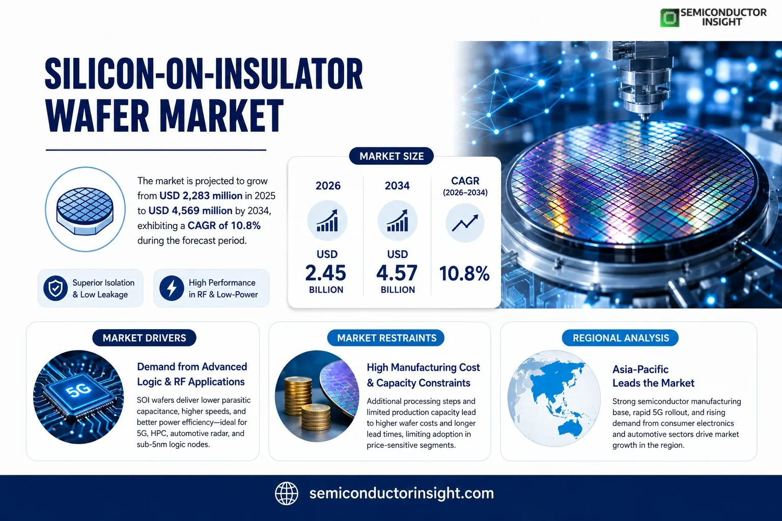
Silicon-on-Insulator Wafer market size was valued at USD 2,283 million in 2025. The market will reach USD 4,569 million by 2034, reflecting a CAGR of 10.8 % over the forecast horizon.
A Silicon‑on‑Insulator wafer consists of a silicon handle substrate, an insulating layer and a thin monocrystalline silicon device layer that serves as the active region for integrated‑circuit fabrication. By electrically isolating devices from the bulk silicon, SOI wafers lower parasitic coupling and capacitance, which translates into stronger isolation, reduced leakage and more reliable operation under demanding RF, low‑power and harsh‑environment conditions.The upward trend stems from high‑frequency connectivity upgrades and tightening energy‑efficiency targets across mainstream semiconductor supply chains. As mobile and wireless standards evolve, RF front‑end designs demand lower insertion loss and higher linearityattributes that SOI substrates readily deliver. Simultaneously, edge‑computing and automotive electronics prioritize low‑voltage operation and dynamic power control; FD‑SOI mechanisms such as enhanced electrostatics and body‑biasing reinforce the case for SOI platforms where designers balance speed against leakage.Nevertheless, cyclical demand swings and lengthy qualification cycles pose risks. Handset‑driven supply chains can trigger inventory corrections that compress short‑term visibility, while engineered substrates require coordinated enablement across foundry platforms, design ecosystems and lead customers. Capital intensity and yield learning curves further elevate barriers for stable scaling through industry cycles.
MARKET DRIVERS
Demand from Advanced Logic Nodes
Silicon-on-Insulator Wafer Market is being propelled by semiconductor manufacturers that are moving to 5‑nm and sub‑5‑nm process nodes. The insulating layer inherent to SOI wafers reduces latch‑up risk and minimizes parasitic capacitance, which translates into higher switching speeds and lower power drawattributes that are critical for high‑performance computing chips. As design teams tighten power budgets, the economic justification for a premium SOI substrate becomes increasingly compelling.
Expansion of RF, Automotive, and 5G Infrastructure
RF front‑end modules for 5G base stations, automotive radar, and millimeter‑wave communications rely on the low‑loss characteristics of SOI. The insulating film curtails substrate noise, enabling tighter integration of active and passive components on a single wafer. With 5G rollout accelerating and automotive manufacturers committing to advanced driver‑assistance systems, the volume of RF‑grade SOI wafers is set to climb sharply.
➤ Analysts note that the premium price differential of SOI wafers is narrowing as larger fab lines achieve economies of scale, thereby widening the addressable market.
Beyond performance, the industry’s shift toward heterogeneous integration amplifies the relevance of SOI technology. By providing a platform that can accommodate logic, memory, and photonic devices simultaneously, SOI wafers help manufacturers reduce package count and shorten time‑to‑marketan advantage that is increasingly prized in a competitive landscape.
MARKET CHALLENGES
Cost Sensitivity in High‑Volume Production
Despite its technical merits, Silicon-on-Insulator Wafer Market confronts price pressure from customers accustomed to bulk‑priced bulk silicon. The additional processing stepssuch as wafer bonding and layer‑transferinflate unit costs by 20‑30 %. For commodity‑driven segments, manufacturers must demonstrate a clear return on investment, or risk being sidelined by cost‑focused design teams.
Other Challenges
Supply Chain Vulnerabilities
The limited number of facilities capable of producing high‑quality SOI wafers creates a concentration risk. Any disruptionwhether from equipment downtime, raw‑material shortages, or geopolitical tensionscan ripple through downstream fab schedules, prompting some customers to revert to conventional silicon as a contingency.
MARKET RESTRAINTS
Manufacturing Capacity Constraints
Only a handful of fabs worldwide possess the dedicated infrastructure required for high‑volume SOI production. The steep capital outlay needed to expand or retrofit existing lines limits the speed at which capacity can be scaled, thereby capping market growth despite rising demand.
MARKET OPPORTUNITIES
Emergence of Heterogeneous Integration Platforms
As chip designers pursue system‑in‑package solutions that blend analog, digital, and photonic functions, SOI wafers are uniquely positioned to serve as the foundational substrate. The insulating layer eases the co‑integration of disparate technologies, opening avenues for new product categories such as AI accelerators and quantum‑interface chips. Companies that can align their process roadmaps with these integration trends stand to capture a sizable share of the next wave of innovation.
Silicon-on-Insulator Wafer Market Trends
RF Performance Gains Elevate Substrate Preference
In Silicon-on-Insulator Wafer Market, the intrinsic isolation between device and bulk silicon translates into measurable reductions in parasitic capacitance. Designers exploiting this characteristic observe lower insertion loss in high‑frequency front‑ends and tighter control of leakage currents in low‑power blocks. The practical outcome is a substrate that supports tighter channel lengths without sacrificing stability, which in turn permits tighter integration of RF filters, power amplifiers, and mixed‑signal blocks on a single die. As mobile standards progress toward wider bandwidths, the marginal improvements in linearity and noise figure afforded by SOI become decisive factors in component selection, prompting OEMs to re‑evaluate baseline wafer choices for upcoming product cycles.
Other Trends
Pricing Pressures and Supply‑Chain Resilience
Typical ex‑works pricing for SOI wafers remains in the US$300‑450 range, while annual shipments hover between 4.5 and 6 million units. This price envelope reflects the additional processing steps required for the buried oxide layer and the tighter yield management needed to maintain uniform device thickness. Because the volume base is modest compared with bulk silicon, any fluctuation in raw‑material costs or lithography capacity quickly ripples through the cost structure. Companies that have cultivated long‑term foundry agreements and diversified their supply sources are better positioned to absorb short‑term inventory corrections that often accompany handset‑driven demand cycles.
Edge Computing and Automotive Expand SOI Application Base
Edge‑oriented processors and automotive electronics demand robust operation under wide temperature swings and strict power envelopes. The Fully‑Depleted SOI (FD‑SOI) variant supplies superior electrostatic control and enables body‑bias techniques that dynamically trade speed for leakage, a capability increasingly valuable in autonomous‑driving modules and industrial control units. As system‑level efficiency targets tighten, platform architects turn to SOI as a means to reduce standby power while preserving high‑frequency performance. However, the longer qualification timelines required for safety‑critical automotive standards and the need for coordinated design‑ecosystem support introduce a layer of risk that firms must manage through early engagement with foundries and IP partners.
COMPETITIVE LANDSCAPEKey Industry Players
Silicon‑on‑Insulator Wafer Market Competitive Overview
Soitec continues to anchor the wafer supply chain, commanding a sizeable share of the 300‑mm segment through its vertically integrated model that couples high‑volume manufacturing with an aggressive R&D pipeline. The French firm’s ability to deliver thin‑film device layers at competitive margins has attracted virtually all major foundries seeking to differentiate RF and FD‑SOI products. Soitec’s recent rollout of 150‑mm and 200‑mm thin‑layer capability widens its addressable market, allowing customers in automotive and edge‑compute domains to adopt SOI without a full redesign of existing fab lines. By aligning wafer pricing with the 300‑450 USD range observed in 2025, the company preserves a cost advantage that smaller niche suppliers struggle to match.Beyond the market leader, a cluster of seasoned manufacturers sustains the ecosystem. Shin‑Etsu Chemical leverages its silicon crystal expertise to service high‑purity 200‑mm orders, while SUMCO supplies bulk silicon substrates that are subsequently bonded into advanced SOI stacks. Foundries, operating both as a fab and a wafer source, bridges design‑to‑silicon hand‑offs for customers pursuing FD‑SOI platforms. Intel and Samsung, although primarily end‑users, have begun internal wafer sourcing to secure supply certainty for their high‑performance compute lines. TSMC, TowerJazz, Bosch Semiconductor, STMicroelectronics, Fujitsu, NXP, and Micron contribute specialized capacityranging from niche 150‑mm runs to bespoke device‑layer thicknessesthereby ensuring that niche applications such as low‑power IoT and ruggedized industrial modules retain access to engineered substrates despite the sector’s cyclical volatility.
List of Key Silicon‑on‑Insulator Wafer Companies Profiled
- Soitec
- Shin‑Etsu Chemical
- SUMCO Corporation
- Foundries
- Intel Corporation
- TSMC
- Samsung Electronics
- TowerJazz (JVCKENWOOD)
- Bosch Semiconductor (Robert Bosch)
- STMicroelectronics
- Fujitsu Semiconductor
- NXP Semiconductors
- Micron Technology
Segment Analysis:
| Segment Category | Sub-Segments | Key Insights |
| By Type |
|
Large wafer format
|
| By Application |
|
RF front‑end modules
|
| By End User |
|
Foundry services
|
| By Technology |
|
Fully depleted SOI (FD‑SOI)
|
| By Performance Requirement |
|
Low‑power operation
|
Regional Analysis: Silicon-on-Insulator Wafer Market
North America
Pioneering fabs in the United States and Canada leverage cutting‑edge lithography to push SOI thickness tolerances, enabling thinner gate oxides and higher drive currents. This technical lead fuels downstream design houses that rely on predictable wafer characteristics for sub‑5nm node roadmaps.
A multi‑tiered supplier base, from silicon boule producers to specialty polishing services, ensures resilience against material shortages. Companies often engage in long‑term contracts, smoothing capacity constraints during peak design cycles.
Alliances between wafer manufacturers and equipment OEMs accelerate co‑development of platform‑specific processes, reducing time‑to‑volume for emerging applications such as quantum‑computing interface chips.
Favorable export‑control policies and clear standards for radiation‑hard SOI devices attract defense contractors, reinforcing a stable demand pipeline for high‑reliability wafers.
Europe
European nations combine strong academic research with a policy environment that emphasizes sustainability. Initiatives across Germany, France, and the Netherlands promote low‑power SOI solutions for green data‑center processors, while the EU’s semiconductor strategy subsidizes pilot lines that explore novel buried‑oxide configurations. This blend of public funding and private expertise creates a niche where design houses can experiment with mixed‑signal platforms without the cost pressures faced in other regions. Consequently, vendors targeting Europe must be agile, offering custom thicknesses and surface‑finish options that match the continent’s emphasis on energy‑efficient hardware.
Asia-Pacific
Asia‑Pacific’s market dynamism stems from a massive manufacturing capacity base coupled with aggressive cost‑optimization drives. Nations such as Taiwan, South Korea, and Singapore host fabs that prioritize volume production of SOI wafers for consumer electronics and mobile communications. At the same time, emerging economies are investing in specialized fabs for automotive and IoT sectors, creating a layered demand structure. The region’s willingness to adopt advanced lithography early offers opportunities for suppliers to introduce next‑generation wafer designs, but it also forces rapid alignment of supply capabilities to avoid bottlenecks during new node introductions.
South America
South American activity remains modest yet strategically focused on niche markets like aerospace and defense, where reliability outweighs cost considerations. Brazil’s defense procurement programs have begun specifying SOI substrates for radiation‑hard sensors, prompting local distributors to secure import channels from established manufacturers. While overall volume is limited, the emphasis on high‑integrity applications encourages vendors to provide tailored support services, such as on‑site technical consultancy and customized packaging, to satisfy the region’s stringent performance criteria.
Middle East & Africa
In the Middle East & Africa, Silicon-on-Insulator Wafer Market is anchored by telecom expansion and nascent smart‑city projects. The United Arab Emirates and Saudi Arabia are channeling sovereign wealth into semiconductor testbeds that explore 5G and edge‑computing deployments, often selecting SOI platforms for their superior signal isolation. Meanwhile, African nations are in the early stages of building digital infrastructure, creating a modest but growing appetite for ruggedized chips. Suppliers that can offer flexible financing and localized technical training are poised to capture the incremental demand emerging from these government‑driven initiatives.
Report Scope
This market research report provides a comprehensive analysis of the Silicon-on-Insulator Wafer Market , covering the forecast period 2026–2034. It offers detailed insights into market dynamics, technological advancements, competitive landscape, and key trends shaping the industry.
Key focus areas of the report include:
- Market Overview: The report begins with an overview outlining its current market scenario, key growth indicators, and industry transformation drivers. It discusses macroeconomic factors, demand–supply balance, regulatory landscape, and the strategic role of semiconductors in powering advancements across industries such as automotive, telecommunications, consumer electronics, and industrial automation.
- Market Size & Forecast: Historical data and future projections for revenue, unit shipments, and market value across major regions and segments.
- Segmentation Analysis: Detailed breakdown by product type, technology, application, and end-user industry to identify high-growth segments and investment opportunities.
- Regional Insights: Insights into market performance across North America, Europe, Asia-Pacific, Latin America, and the Middle East & Africa, including country-level analysis where relevant.
- Competitive Landscape: Profiles of leading market participants, including their product offerings, R&D focus, manufacturing capacity, pricing strategies, and recent developments such as mergers, acquisitions, and partnerships.
- Technology Trends & Innovation: Assessment of emerging technologies, integration of AI/IoT, semiconductor design trends, fabrication techniques, and evolving industry standards.
- Market Drivers & Restraints: Evaluation of factors driving market growth along with challenges, supply chain constraints, regulatory issues, and market-entry barriers.
- Stakeholder Insights: Insights for component suppliers, OEMs, system integrators, investors, and policymakers regarding the evolving ecosystem and strategic opportunities.
Primary and secondary research methods are employed, including interviews with industry experts, data from verified sources, and real-time market intelligence to ensure the accuracy and reliability of the insights presented.
FREQUENTLY ASKED QUESTIONS:
What is the current market size of Silicon-on-Insulator Wafer Market?
-> Silicon-on-Insulator Wafer Market was valued at USD 2283 million in 2025 and is expected to reach USD 4569 million by 2034 with a CAGR of 10.8%.
Which key companies operate in Silicon-on-Insulator Wafer Market?
-> Key players include major semiconductor manufacturers and foundries developing SOI technology, such as Intel, Foundries, STMicroelectronics, TSMC, and Samsung.
What are the key growth drivers?
-> Key growth drivers include high‑frequency connectivity upgrades, energy‑efficiency demands, edge computing, automotive and industrial electronics requiring low‑power and robust performance.
Which region dominates the market?
-> Asia‑Pacific is the fastest‑growing region, while North America remains a dominant market due to its strong semiconductor manufacturing base.
What are the emerging trends?
-> Emerging trends include increased adoption of FD‑SOI for advanced low‑power applications, integration of body‑biasing techniques, and expanded use in 5G RF front‑ends.
Get Sample Report PDF for Exclusive Insights
Report Sample Includes
- Table of Contents
- List of Tables & Figures
- Charts, Research Methodology, and more...
 Download Sample Report PDF



