Semiconductor Bonding Capillaries Market Insights
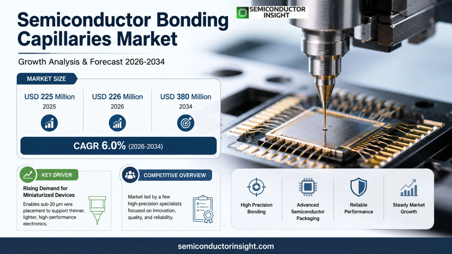
Semiconductor Bonding Capillaries market size was valued at USD 225 million in 2025. The market is projected to grow from USD 226 million in 2026 to approximately USD 380 million by 2034, exhibiting a CAGR of about 6.0% during the forecast period.
Semiconductor Bonding Capillaries are precision consumables used in wire‑bonding during semiconductor packaging. Typically forged from high‑hardness ceramics or tungsten carbide, they feature an inner hole sized to match wire diameter, a flare/chamfer for guidance, and a tip geometry that delivers controlled pressure, temperature and ultrasonic vibration to form reliable interconnects.
The market expands because rising chip shipments for AI, HPC, IoT and 5G increase demand for reliable wire‑bonding tools, while cost‑effective traditional bonding remains dominant despite emerging flip‑chip techniques. However, finer pitch requirements and higher bonding temperatures push manufacturers toward advanced zirconia‑alumina composites and tighter tolerances, creating both opportunities and technical challenges.
MARKET DRIVERS
Rising Demand for Miniaturized Devices
The push toward thinner, lighter consumer electronics forces chip manufacturers to adopt finer interconnects. Semiconductor Bonding Capillaries enable the placement of sub‑20 µm wires, a capability that directly supports the form‑factor ambitions of flagship smartphones and wearables. As design cycles tighten, suppliers that can guarantee sub‑micron positional accuracy gain a competitive edge.
Advances in Wire‑Bonding Automation
Modern bonding tools now integrate vision‑guided alignment and real‑time force feedback. These features reduce cycle time by up to 15 % while maintaining defect rates below 0.02 %. Capillary manufacturers that embed sensor data interfaces into their products are seeing accelerated adoption among fabs that prioritize throughput.
➤ “Customers are willing to pay a premium for capillaries that deliver consistent loop height and minimize re‑work, especially when yield penalties exceed $500 per wafer.”
Beyond speed, the shift toward high‑frequency signaling imposes stricter impedance control. The geometry of the capillary tip, combined with optimized coating materials, directly influences signal integrity. Firms that invest in proprietary alloy formulations can capture premium segments that value performance over cost.
MARKET CHALLENGES
Manufacturing Yield Sensitivity
Even marginal variations in tip diameter can translate into measurable yield loss across large volumes. When a single defective capillary contaminates a batch, the resulting re‑work can erode profit margins by several percentage points. Vendors must therefore adhere to tight tolerance windows and implement rigorous in‑process inspection.
Other Challenges
Material Compatibility Issues
The push for lead‑free and environmentally compliant alloys has introduced new intermetallic formation patterns. Some emerging coatings react unfavorably with high‑temperature solder pastes, prompting additional qualification cycles that delay time‑to‑market.
MARKET RESTRAINTS
Regulatory Oversight on Chemical Use
Global agencies increasingly restrict the use of certain flux chemicals and surface‑treatment solvents in capillary production. Compliance audits add operational overhead, and non‑conforming batches risk costly recalls. Manufacturers that lack a robust chemical‑management system may find market entry slowed.
MARKET OPPORTUNITIES
Emergence of 3D Integrated Packages
Three‑dimensional stacking technologies require ultra‑precise wire placement to connect vertically integrated dies. Semiconductor Bonding Capillaries Market participants that tailor tip designs for through‑silicon vias (TSVs) stand to benefit from the projected expansion of heterogeneous integration. Early adopters can lock in strategic partnerships with leading package houses.
Semiconductor Bonding Capillaries Market Trends
Rising Demand from Advanced Packaging
The surge in high‑performance computing, artificial‑intelligence accelerators, Internet‑of‑Things devices and 5G infrastructure has deepened the need for fine‑pitch wire bonding. In 2024 manufacturers shipped roughly 53.38 million capillaries, with an average transaction price of US$ 4.62 per unit. This volume reflects the continued reliance on wire bonding for power‑device and memory‑chip production, where cost efficiency and proven reliability outweigh the allure of emerging flip‑chip techniques. The forecast for 2032 places total market revenue at about US$ 346 million, up from US$ 225 million in 2025, indicating that the industry is set to expand while retaining a price‑point that supports high‑volume adoption across Tier‑1 fabs.
Other Trends
Material Innovation and Tool Longevity
Manufacturers are responding to tighter geometric tolerances by shifting from conventional tungsten carbide toward composite zirconia‑alumina ceramics. These blends deliver superior wear resistance and thermal stability, crucial for handling copper wires whose hardness stresses tool surfaces. By tightening the corner‑radius design and refining inner‑hole geometry, suppliers can extend capillary life cycles, reducing downtime for re‑tooling and preserving process yield on high‑density interconnects.
Regional Shifts and Supply‑Chain Localization
Asia‑Pacific accounts for the bulk of both consumption and production, anchored by extensive OSAT clusters in China, Taiwan, South Korea and Southeast Asia. Recent policy incentives aimed at localizing semiconductor supply chains have encouraged domestic manufacturers to invest in high‑purity ceramic processing and precision machining. While Japanese, U.S. and European firms continue to dominate the premium segment, Chinese and other Asian players are capturing a growing share of the mid‑range market by offering competitive pricing without sacrificing dimensional accuracy. This realignment suggests that future market share will hinge on the ability of regional suppliers to match the performance standards of established leaders while leveraging cost advantages.
COMPETITIVE LANDSCAPE
Key Industry Players
Semiconductor Bonding Capillaries – Competitive Overview
The market is anchored by a handful of technologically sophisticated firms that dominate the high‑precision segment. K&S (USA) leverages decades‑long expertise in tungsten‑carbide tooling and commands premium pricing through a portfolio of ultra‑fine pitch capillaries that meet sub‑micron hole‑diameter tolerances demanded by AI‑focused packaging lines. In parallel, Japan’s SPT and Orbray supply ceramic‑based solutions that combine zirconia‑alumina composites with proprietary heat‑treatment cycles, delivering superior wear resistance for copper wire bonding applications. These leaders retain tightly held relationships with Tier‑1 OSATs and major fabless designers, which translates into recurring volume contracts and a defensible share of the $346 million market projected for 2032.
Beyond the top tier, a dozen regional manufacturers have carved out niches by emphasizing cost‑effective production and rapid engineering cycles. PECO (Germany) excels in modular capillary families tailored for mid‑range memory modules, while KOSMA (Germany) differentiates through a flexible design‑for‑manufacturability approach that shortens time‑to‑market for new hole‑diameter specifications. Megtas (France) and TOTO (Taiwan) focus on high‑temperature ceramic grades that serve power‑electronics platforms. Chinese entrants such as Dou Yee Enterprises, Sunbelt Semi, ChaoZhou Three‑Circle (Group) and Xinhe Semicon have expanded capacity in the APAC hub, leveraging local supply chains to undercut imports on standard‑spec products. Suntech (South Korea) rounds out the list with a hybrid ceramic‑metal capillary line that addresses the growing demand for 5G and automotive modules.
List of Key Semiconductor Bonding Capillaries Companies Profiled
- K&S
- K&S
- SPT
- SPT
- PECO
- KOSMA
- Megtas
- TOTO
- Orbray
- Dou Yee Enterprises
- Sunbelt Semi
- ChaoZhou Three-Circle (Group)
- Suntech
- Xinhe Semicon
Segment Analysis:
| Segment Category | Sub-Segments | Key Insights |
| By Type |
|
Gold Wire Capillaries
|
| By Application |
|
Semiconductor Packaging
|
| By End User |
|
Packaging Service Providers
|
| By Material |
|
Ceramic (Zirconia‑Alumina composites)
|
| By Hole Diameter |
|
30‑100 µm (Fine‑Pitch)
|
Regional Analysis: Semiconductor Bonding Capillaries Market
North America
The Pacific Northwest and Midwest host clusters devoted to 2.5 D/3 D integration, where bonding capillaries become a critical conduit for fine‑pitch interconnects. Companies exploit localized supplier networks to shorten design cycles, allowing rapid iteration on capillary tip profiles that suit heterogeneous integration. This proximity fuels a feedback loop: production challenges spur material refinements, which in turn unlock denser package architectures.
Recent disruptions highlighted the advantage of diversified sourcing for glass preforms and precision machining services. Firms have embraced dual‑sourcing models, pairing domestic mills with select overseas partners to mitigate lead‑time volatility. This strategic offsetting reduces the risk of bottlenecks that could otherwise impede capillary availability for high‑mix, low‑volume production runs.
University research centers in California and Texas receive sustained grants aimed at microscale fluid dynamics, directly feeding intellectual property back to equipment manufacturers. Collaborative consortia often publish breakthroughs on surface‑tension control, enabling capillaries that dispense solder paste with unprecedented uniformity, a factor that device designers now weigh alongside traditional electrical performance metrics.
While the United States does not impose explicit standards on bonding capillaries, compliance with broader environmental and safety directives influences material selection. Companies that proactively adopt low‑emission glass formulations gain smoother access to automotive and medical device certification pathways, strengthening their market positioning.
Europe
European semiconductor assemblers place a premium on precision engineering, and this cultural focus reverberates through the regional bonding capillaries market. Nations such as Germany and the Netherlands host a network of specialist glass producers that emphasize ultra‑cleanroom compatibility, catering to customers who must meet stringent EU environmental directives. Collaborative projects funded through Horizon Europe align material scientists with equipment builders, accelerating the rollout of capillaries with tailored thermal expansion coefficients. The continent’s strong emphasis on sustainability pushes suppliers toward recyclable glass blends, a trend that resonates with automotive OEMs targeting lower carbon footprints. Collectively, these dynamics reinforce Europe’s reputation for quality‑driven, environmentally conscious solutions.
Asia‑Pacific
Asia‑Pacific economies, led by Taiwan, South Korea, and China, generate the bulk of global wafer output, and their rapid adoption of advanced packaging fuels demand for sophisticated bonding capillaries. Local manufacturers benefit from high‑volume production scales, which encourage incremental refinements in tip geometry to accommodate ever‑smaller pitch sizes. Government incentives that target “silicon‑on‑everything” strategies have spurred joint ventures between capillary makers and fab operators, fostering co‑development of bespoke solutions. Although price sensitivity remains pronounced, the willingness to invest in higher‑performance capillaries when they demonstrably improve defect‑free yields distinguishes the region’s approach from purely cost‑driven markets.
South America
South American participation in Semiconductor Bonding Capillaries market is modest but evolving. Brazil’s growing electronics manufacturing base has begun to import specialized capillaries for niche applications such as renewable‑energy converters and aerospace components. Local distributors are building technical expertise, offering on‑site training that reduces reliance on overseas support. While the market share remains limited, the region’s focus on building indigenous capabilities hints at a gradual shift toward more self‑sufficient supply chains, especially as regional trade agreements promote technology transfer.
Middle East & Africa
The Middle East and Africa exhibit a nascent yet increasingly strategic interest in semiconductor packaging technologies. In the United Arab Emirates, government‑backed accelerators are nurturing startups that explore novel glass compositions for capillaries, positioning the country as a potential hub for downstream tooling services. Meanwhile, African nations with emerging electronics assemblage sectors are looking to import capillaries that meet rigorous reliability criteria for telecommunications infrastructure. The overarching narrative is one of cautious entry, with stakeholders emphasizing capacity building and alignment with global quality standards to attract multinational investment.
Report Scope
This market research report provides a comprehensive analysis of the Semiconductor Bonding Capillaries Market , covering the forecast period 2026–2034. It offers detailed insights into market dynamics, technological advancements, competitive landscape, and key trends shaping the industry.
Key focus areas of the report include:
- Market Overview: The report begins with an overview outlining its current market scenario, key growth indicators, and industry transformation drivers. It discusses macroeconomic factors, demand–supply balance, regulatory landscape, and the strategic role of semiconductors in powering advancements across industries such as automotive, telecommunications, consumer electronics, and industrial automation.
- Market Size & Forecast: Historical data and future projections for revenue, unit shipments, and market value across major regions and segments.
- Segmentation Analysis: Detailed breakdown by product type, technology, application, and end-user industry to identify high-growth segments and investment opportunities.
- Regional Insights: Insights into market performance across North America, Europe, Asia-Pacific, Latin America, and the Middle East & Africa, including country-level analysis where relevant.
- Competitive Landscape: Profiles of leading market participants, including their product offerings, R&D focus, manufacturing capacity, pricing strategies, and recent developments such as mergers, acquisitions, and partnerships.
- Technology Trends & Innovation: Assessment of emerging technologies, integration of AI/IoT, semiconductor design trends, fabrication techniques, and evolving industry standards.
- Market Drivers & Restraints: Evaluation of factors driving market growth along with challenges, supply chain constraints, regulatory issues, and market-entry barriers.
- Stakeholder Insights: Insights for component suppliers, OEMs, system integrators, investors, and policymakers regarding the evolving ecosystem and strategic opportunities.
Primary and secondary research methods are employed, including interviews with industry experts, data from verified sources, and real-time market intelligence to ensure the accuracy and reliability of the insights presented.
FREQUENTLY ASKED QUESTIONS:
What is the current market size of Semiconductor Bonding Capillaries Market?
-> Semiconductor Bonding Capillaries market is projected to grow from USD 226 million in 2026 to approximately USD 380 million by 2034, a CAGR of about 6.0%
Which key companies operate in Semiconductor Bonding Capillaries Market?
-> Key players include K&S, SPT, PECO, KOSMA, Megtas, TOTO, Orbray, Dou Yee Enterprises, Sunbelt Semi, ChaoZhou Three-Circle (Group), Suntech, Xinhe Semicon.
What are the key growth drivers?
-> Key growth drivers include the rapid expansion of the global semiconductor packaging market driven by high‑performance computing, artificial intelligence, IoT and 5G, the cost‑effectiveness and maturity of wire‑bonding technology, and increasing demand for power‑device and memory applications.
Which region dominates the market?
-> Asia-Pacific remains the largest consumer and production hub, supported by dense OSAT clusters in China, Taiwan, South Korea and Southeast Asia.
What are the emerging trends?
-> Emerging trends include shifts toward fine‑pitch packaging requiring sub‑micron hole diameters, the adoption of advanced composite zirconia‑alumina ceramics for higher temperature and ultrasonic power resistance, innovation in copper‑wire bonding tools, and increasing localization of the semiconductor supply chain in Asian markets.

Get Sample Report PDF for Exclusive Insights
Report Sample Includes
- Table of Contents
- List of Tables & Figures
- Charts, Research Methodology, and more...
 Download Sample Report PDF