
Atomic Layer Deposition for Display Market Insights
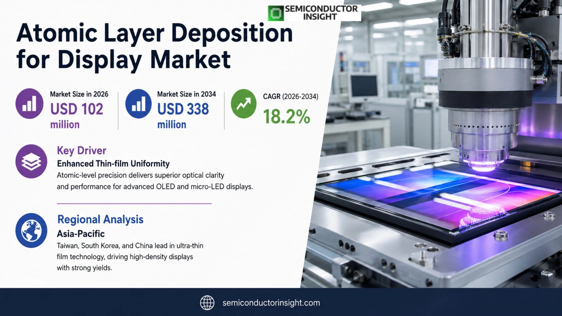
Atomic Layer Deposition for Display market is forecasted to rise from USD 102 million in 2026 to USD 338 million by 2034, exhibiting a CAGR of 18.2% over the period.
Atomic Layer Deposition for Display (Display‑ALD) refers to the use of atomic‑layer‑deposition technology in the manufacture of display panels, enabling deposition of nanoscale functional thin films on glass or flexible substrates with atomic‑level thickness control and high uniformity.
The expansion is linked to increasing demand for high‑performance thin‑film encapsulation in flexible OLEDs, growing adoption of Mini‑LED and Micro‑LED architectures that require precise pixel‑level dielectric layers, and concentration of new production lines in Asia. Recent activity includes a partnership announced in March 2024 between Applied Materials and a leading OLED manufacturer to co‑develop high‑throughput ALD tools, while companies such as Qingdao Sirui Intelligent Technology and Oxford Instruments have launched next‑generation spatial ALD systems targeting large‑area substrates.
MARKET DRIVERS
Enhanced Thin‑film Uniformity
Atomic Layer Deposition for Display market thrives on its capacity to lay down conformal layers with atomic‑scale precision. This level of control translates into higher optical clarity and improved carrier mobility for OLED and micro‑LED panels, directly influencing yield and end‑product reliability.
Cost‑effective Scaling for Large‑area Panels
Recent equipment upgrades enable continuous‑flow reactors that cover glass substrates exceeding 300 mm. Manufacturers can now apply protective and functional layers in a single pass, reducing batch‑changeover time and lowering capital intensity per square meter.
➤ The ability to deposit sub‑nanometer layers across 8‑K glass has shortened product cycles and opened new form‑factor possibilities.
As design cycles tighten, early‑stage integration of ALD into the fab line becomes a decisive factor for companies seeking to differentiate through brightness, color gamut, and longevity.
MARKET CHALLENGES
Technology Integration Complexity
Integrating ALD tools with existing thin‑film deposition lines demands synchronized process control and sophisticated software interfaces. Companies that overlook the learning curve risk bottlenecks that offset the material advantages.
Other Challenges
Supply Chain Constraints
The specialized precursors required for high‑purity layers are sourced from a limited set of vendors. Any disruption,whether geopolitical or logistical,can inflate input costs and delay production schedules.
MARKET RESTRAINTS
High Initial Capital Outlay
Despite declining unit prices for ALD reactors, the cumulative investment for a full‑scale display line,including vacuum chambers, precursor handling, and in‑line metrology,remains a barrier for midsize manufacturers aiming to upgrade their technology stack.
MARKET OPPORTUNITIES
Emerging Flexible and Foldable Displays
The move toward bendable and rollable screens creates demand for ultra‑thin barrier layers that can endure repeated mechanical stress. ALD’s ability to produce pin‑hole‑free films at low temperature makes it uniquely positioned to supply these next‑generation form factors.
Moreover, the push for higher pixel densities in AR/VR headsets hinges on precise optical coatings that preserve luminance while minimizing parasitic reflections. Companies that can leverage ALD’s conformality are likely to capture a premium segment of the immersive‑device supply chain.
Finally, sustainability pressures are encouraging OEMs to adopt processes with reduced waste. ALD’s self‑limiting chemistry delivers near‑100 % material utilization, aligning operational cost savings with environmental commitments.
Atomic Layer Deposition for Display Market Trends
ALD Adoption Accelerates in Flexible OLED
The shift toward foldable and rollable screens forces panel makers to address water‑oxygen ingress with unprecedented rigor. Atomic Layer Deposition delivers a barrier that can be tuned atom‑by‑atom, guaranteeing the sub‑nanometer uniformity essential for maintaining luminance stability on a bending substrate. As original equipment manufacturers embed these layers into the encapsulation workflow, the cost premium is justified by the extension of product lifetime and the avoidance of premature failure modes that would otherwise erode brand reputation. Consequently, Atomic Layer Deposition for Display market is witnessing a reallocation of capital from legacy CVD/PVD lines toward ALD‑specific reactors that can service large‑area glass and flexible polymers alike.
Other Trends
Mini‑LED & Micro‑LED Integration
Mini‑LED back‑lights and emerging Micro‑LED arrays rely on pixel‑level dielectric films to control crosstalk and to protect individual emitters from environmental stress. The precision of ALD enables a dielectric thickness that balances optical performance with thermal management, a trade‑off that conventional techniques struggle to meet. Suppliers that can marry high‑throughput batch systems with the spatial uniformity demanded by high‑resolution panels are seeing increased order volumes, especially from automotive OEMs that prioritize reliability under extreme temperature cycles.
Supply‑Chain Consolidation Strengthens Market Position
Upstream, the scarcity of ultra‑pure precursors has prompted a handful of specialty chemical firms to secure exclusive contracts with the midstream equipment manufacturers. This vertical integration reduces variability in film quality and shortens the qualification timeline for new display architectures. Downstream, panel assemblers in Asia are clustering production in megafabs that host dedicated ALD stations, creating economies of scale that lower the per‑unit equipment amortization. The resulting ecosystem,tightened material sourcing, standardized process modules, and shared analytics platforms,makes Atomic Layer Deposition for Display market more resilient to supply shocks while delivering a gross margin profile that hovers in the 40‑50 % band.
COMPETITIVE LANDSCAPE
Key Industry Players
Atomic Layer Deposition for Display: Competitive Overview
Applied Materials continues to dominate the Display‑ALD arena, leveraging its extensive equipment portfolio and deep integration capabilities to secure a sizeable share of the 80‑unit global capacity. Its thermal and spatial ALD platforms are favored by large‑scale OLED and emerging Micro‑LED fabs because of proven reliability and the ability to process 300‑mm glass sheets. The company’s vertical approach,covering precursor sourcing, software control, and after‑sales service,creates a high barrier to entry and forces midsize firms to specialize in niche equipment or process development. Meanwhile, regional players such as SK hynix’s ALD division and Taiwan‑based ASM Pacific Technology are carving out market segments focused on flexible‑display encapsulation, where thin‑film uniformity across bendable substrates is paramount. The overall structure points to a tiered ecosystem: a handful of multinational OEMs command the bulk of mass‑production lines, while a vibrant second tier supplies customized solutions for specialized applications and pilot‑scale projects.
Beyond the headline names, the niche tier includes a mix of seasoned equipment vendors and emerging specialists. Qingdao Sirui Intelligent Technology and Jiangsu Leadmicro Nano Technology provide cost‑effective batch systems that attract smaller panel makers in Southeast Asia. European outfits such as Oxford Instruments and NCD supply precision research‑grade ALD tools that feed process‑development labs, ensuring a pipeline of innovation for next‑generation barrier films. Asian innovators like Skytech Inc and Optorun Semiconductor Technology are expanding into spatial‑ALD configurations tailored to high‑throughput Mini‑LED production. The diversity of these players underscores a competitive environment where differentiation rests on precursor chemistry expertise, system scalability, and the ability to co‑develop process recipes with display manufacturers.
List of Key Atomic Layer Deposition for Display Companies Profiled
- Applied Materials
- Qingdao Sirui Intelligent Technology Co., Ltd
- Jusung Engineering
- ASM Pacific Technology
- CN1
- Jiangsu Leadmicro Nano Technology Co., Ltd
- XIAMEN YUNMAO
- Skytech Inc
- Oxford Instruments
- NCD
- Optorun Semiconductor Technology
- SK hynix ALD Division
Segment Analysis:
| Segment Category | Sub-Segments | Key Insights |
| By Type |
|
Production ALD Equipment
|
| By Application |
|
OLED
|
| By End User |
|
Smartphones
|
| By Technology |
|
Spatial ALD System
|
| By Material |
|
Oxide ALD
|
Regional Analysis: Atomic Layer Deposition for Display Market
High‑volume LCD and OLED fabs cluster around the Taiwan‑Korea corridor, where plant upgrades frequently incorporate atomic‑layer tools to meet tighter tolerance specifications. The concentration of expertise drives rapid diffusion of best practices across the supply chain.
Government‑backed programs in Japan and China channel sizable budgets into thin‑film research, encouraging collaborations between universities and equipment vendors that accelerate process breakthroughs.
The region’s engineering schools churn out specialists versed in surface chemistry and vacuum engineering, providing a steady pipeline of talent that sustains equipment manufacturers and end‑users alike.
Strategic road‑maps emphasize high‑resolution displays for next‑gen devices, prompting subsidies and tax reliefs that lower capital outlays for atomic‑layer deposition installations.
North America
In the United States, Atomic Layer Deposition for Display market is largely driven by a mix of legacy LCD manufacturers and a fast‑growing micro‑LED niche. Companies invest heavily in pilot lines to validate new stack architectures, often in partnership with university research centers. The emphasis on premium‑grade smartphones and automotive heads‑up displays creates a demand for highly uniform films, prompting equipment suppliers to tailor solutions for low‑temperature processes. While the overall volume is smaller than Asia‑Pacific, the willingness to adopt cutting‑edge process controls gives North America a reputation for quality‑focused innovation.
Europe
European stakeholders focus on sustainability and circular‑economy principles, shaping the adoption of atomic‑layer techniques that minimize material waste. German and French display equipment firms are leveraging the technology to meet stringent environmental regulations while targeting high‑end television and professional monitor markets. Collaborative consortia between research institutes and OEMs accelerate standardization of precursor chemistries, enhancing cross‑border supply chain resilience. The region’s strength lies in its ability to blend precision engineering with eco‑conscious design, positioning Europe as a niche but influential player.
South America
South American activity centers on refurbishing existing LCD capacity and exploring cost‑effective OLED pathways. Brazil’s emerging display ecosystem relies on technology transfer agreements, bringing atomic‑layer expertise from abroad to improve panel uniformity. Consumers’ demand for affordable high‑definition screens fuels a pragmatic approach: incremental upgrades rather than wholesale equipment overhauls. This measured adoption strategy helps local manufacturers stay competitive without incurring prohibitive capital costs.
Middle East & Africa
In the Middle East and Africa, market momentum is modest but growing, propelled by regional initiatives to diversify economies beyond oil and minerals. Investment funds earmarked for advanced manufacturing are beginning to allocate resources toward display fabs that incorporate atomic‑layer deposition for niche applications such as premium signage and defense‑grade optics. Partnerships with Asian equipment suppliers provide a technology bridge, while local universities nurture a small but skilled workforce capable of supporting pilot projects. The trajectory suggests a gradual build‑out that could introduce new demand pockets over the next decade.
Report Scope
This market research report provides a comprehensive analysis of the Atomic Layer Deposition for Display Market , covering the forecast period 2026–2034. It offers detailed insights into market dynamics, technological advancements, competitive landscape, and key trends shaping the industry.
Key focus areas of the report include:
- Market Overview: The report begins with an overview outlining its current market scenario, key growth indicators, and industry transformation drivers. It discusses macroeconomic factors, demand–supply balance, regulatory landscape, and the strategic role of semiconductors in powering advancements across industries such as automotive, telecommunications, consumer electronics, and industrial automation.
- Market Size & Forecast: Historical data and future projections for revenue, unit shipments, and market value across major regions and segments.
- Segmentation Analysis: Detailed breakdown by product type, technology, application, and end-user industry to identify high-growth segments and investment opportunities.
- Regional Insights: Insights into market performance across North America, Europe, Asia-Pacific, Latin America, and the Middle East & Africa, including country-level analysis where relevant.
- Competitive Landscape: Profiles of leading market participants, including their product offerings, R&D focus, manufacturing capacity, pricing strategies, and recent developments such as mergers, acquisitions, and partnerships.
- Technology Trends & Innovation: Assessment of emerging technologies, integration of AI/IoT, semiconductor design trends, fabrication techniques, and evolving industry standards.
- Market Drivers & Restraints: Evaluation of factors driving market growth along with challenges, supply chain constraints, regulatory issues, and market-entry barriers.
- Stakeholder Insights: Insights for component suppliers, OEMs, system integrators, investors, and policymakers regarding the evolving ecosystem and strategic opportunities.
Primary and secondary research methods are employed, including interviews with industry experts, data from verified sources, and real-time market intelligence to ensure the accuracy and reliability of the insights presented.
FREQUENTLY ASKED QUESTIONS:
What is the current market size of Atomic Layer Deposition for Display Market?
-> Atomic Layer Deposition for Display market is forecasted to rise from USD 102 million in 2026 to USD 338 million by 2034, exhibiting a CAGR of 18.2%
Which key companies operate in Atomic Layer Deposition for Display Market?
-> Key players include Qingdao Sirui Intelligent Technology Co., Ltd, Jusung Engineering, Applied Materials, CN1, Jiangsu Leadmicro Nano Technology Co., Ltd, XIAMEN YUNMAO, Skytech Inc, Oxford Instruments, NCD, Optorun Semiconductor Technology, among others.
What are the key growth drivers?
-> Key growth drivers include the rapid expansion of flexible and foldable OLED displays demanding high‑performance thin‑film encapsulation, the industrialization of Mini‑LED and Micro‑LED technologies requiring pixel‑level consistency, and the concentration of display manufacturing capacity in Asia accelerating ALD equipment adoption.
Which region dominates the market?
-> Asia dominates the market, driven by extensive OLED, Mini‑LED and Micro‑LED production facilities, while the region also leads in ALD equipment deployment.
What are the emerging trends?
-> Emerging trends include the shift of ALD from niche high‑end packaging to broader functional layers across flexible, foldable and next‑generation high‑performance display panels, and increased integration of ALD processes in mass‑production lines for OLED, Mini‑LED and Micro‑LED technologies.

Get Sample Report PDF for Exclusive Insights
Report Sample Includes
- Table of Contents
- List of Tables & Figures
- Charts, Research Methodology, and more...
 Download Sample Report PDF


