Resist Processing Systems Market Insights
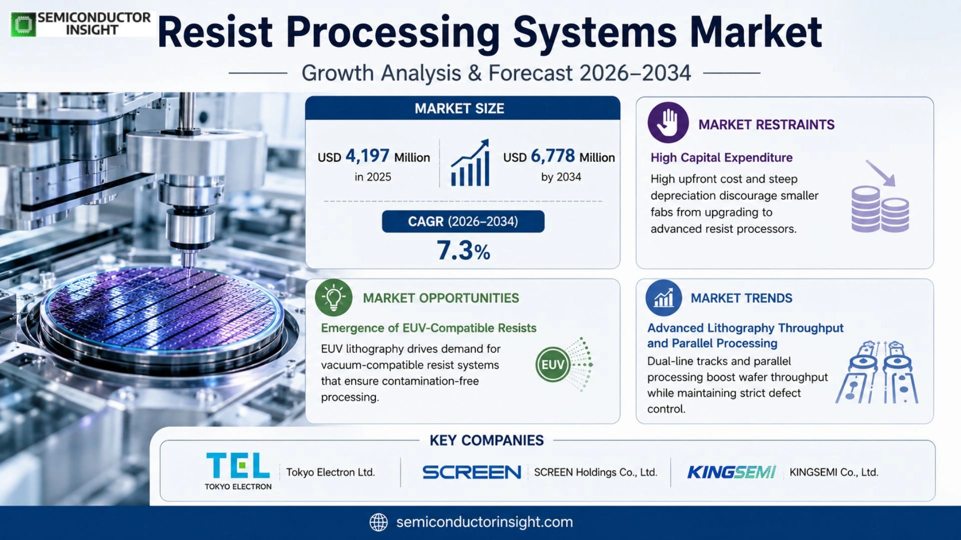
Resist Processing Systems market size was valued at USD 4,197 million in 2025 and will reach USD 6,778 million by 2034, reflecting a CAGR of 7.3% over the forecast period.
Resist Processing Systems refer to integrated coat/develop “track” tools (coater/developer, wafer track) positioned beside a stepper or scanner within a lithography cell to carry out the sequential resist‑processing flow that enables pattern transfer. In practice, a resist track combines modular functions such as spin or spray coating, edge‑bead removal (EBR), soft bake / post‑exposure bake (PEB) / chill conditioning, puddle or spray developing, rinse/dry stages, buffering and robotic wafer handling together with FOUP/load‑port interfaces and alignment modules designed to match scanner takt time. Tokyo Electron’s annual report describes the coater/developer as the system that coats and develops wafers with photoresist while operating in concert with the exposure tool.
The market expands because of heightened capital spending on semiconductor lithography equipment, growing demand for high‑throughput 300 mm multi‑module tracks and the need for tighter defect control as EUV and High‑NA nodes mature. Suppliers such as TEL have introduced CLEAN TRACK™ LITHIUS series with enhanced OEE and lower cost of ownership, while SCREEN’s DT‑3000 (SOKUDO DUO) offers dual parallel lines that raise throughput for immersion ArF and e‑beam applications. Emerging players from China and SEMES are also adding capacity, reinforcing supply‑chain resilience across regions.
MARKET DRIVERS
Technology Adoption in Advanced Lithography
Manufacturers of semiconductors are integrating more sophisticated resist processing workflows to meet the dimensional tolerances demanded by sub‑10 nm node devices. This shift forces equipment suppliers to refine coating uniformity and develop low‑scratch formulations, thereby stimulating demand for Resist Processing Systems market.
Cost‑Efficiency Pressures
Foundries are under pressure to reduce per‑wafer expenditures while maintaining yield. Modern resist processing platforms that combine multi‑track alignment with inline metrology enable tighter cycle times, translating into measurable savings that justify capital allocation.
➤ Firms that can deliver a 15 % reduction in cycle time while preserving defect density are rapidly gaining preference among high‑volume producers.
Because yield improvement directly impacts revenue, investment in next‑generation resist processors is being treated as a strategic lever rather than a discretionary expense, cementing Resist Processing Systems market as a vital component of contemporary fab strategies.
MARKET CHALLENGES
Complexity of Multi‑Layer Integration
As device architectures evolve toward heterogeneous integration, the number of resist layers per wafer is climbing. Managing cross‑contamination and maintaining critical dimension control across diverse materials increases process complexity, raising the barrier for entry for new equipment vendors.
Other Challenges
Skilled Workforce Shortage
The specialized knowledge required to operate and maintain high‑precision resist processing lines is scarce, prompting fabs to invest heavily in training programs or to outsource certain steps, which can dilute the perceived advantage of in‑house systems.
Regulatory scrutiny over chemical usage adds another layer of difficulty, as compliance with emerging environmental standards forces manufacturers to reassess solvent compositions and waste‑handling protocols.
MARKET RESTRAINTS
High Capital Expenditure
Initial outlay for state‑of‑the‑art resist processors often exceeds the budget thresholds of smaller fabs, prompting them to postpone upgrades despite clear efficiency gains. The steep depreciation schedule further discourages rapid fleet turnover.
Additionally, the long qualification cycles associated with new resist chemistries can stall adoption, as manufacturers prefer proven lines to avoid production disruptions.
These financial and operational frictions act as a ceiling on the pace at which Resist Processing Systems market can expand across the broader semiconductor ecosystem.
MARKET OPPORTUNITIES
Emergence of EUV‑Compatible Resists
The transition to extreme ultraviolet lithography creates a niche for resist processing platforms that can handle EUV‑sensitive formulations without introducing contamination. Suppliers that engineer vacuum‑compatible toolchains stand to capture a sizable share of upcoming fab investments.
Parallel advances in AI‑driven process optimization present another growth vector. By embedding predictive analytics within resist processors, vendors can offer adaptive control loops that continuously fine‑tune exposure parameters, delivering higher yields with minimal operator intervention.
Finally, expanding demand from specialty sectors such as quantum‑computing chips and advanced sensor arrays introduces tailored resist processing requirements, opening avenues for customized system offerings within Resist Processing Systems market.
Resist Processing Systems Market Trends
Advanced Lithography Throughput and Parallel Processing
The broader evolution of Resist Processing Systems market is reshaping equipment design around productivity pressure on lithography cells. Equipment makers such as Tokyo Electron and SCREEN have introduced dual‑line tracks that double wafer‑per‑hour capability while preserving tight defect budgets. The additional line allows simultaneous coat‑develop cycles, matching the decreasing takt time of high‑NA EUV scanners. Customers report that the extra throughput translates into higher fab utilization and lower per‑chip cost, especially in logic and high‑density memory fabs where scanner time commands a premium. This shift toward parallelism is reinforced by tighter thermal stability requirements; dual‑line architectures spread heat loads, reducing wafer‑temperature drift that would otherwise impair critical dimension control. Moreover, the modular footprint eases integration into existing cleanrooms, enabling incremental upgrades without major layout changes. The overall effect is a measurable lift in overall equipment effectiveness, strengthening the business case for capital allocation to next‑generation lithography.
Other Trends
Supply‑Chain Localization and Second‑Source Emergence
Geopolitical pressures and recent shortages have prompted semiconductor manufacturers to diversify their equipment base. Domestic suppliers in China and emerging Korean players are now field‑testing ArF‑i photo‑processing tracks that claim comparable uptime to established Japanese and European models. This emergence of second‑source options reduces reliance on a single vendor and shortens lead times, a factor that many fabs cite when planning capacity expansions. The trend also spurs competitive pricing, as incumbents introduce cost‑of‑ownership improvements to retain market share. For equipment integrators, the need to certify new tools across a broader set of scanner interfaces creates opportunities for software upgrades and standardized data pipelines.
Material Diversification and Packaging Integration
Beyond traditional photoresist, customers are demanding tracks that handle polymer‑based hard masks, bottom‑anti‑reflective coatings, and spin‑on die‑attach layers. Platform vendors have responded by adding interchangeable coating heads, variable‑temperature bake modules, and solvent‑recovery loops that accommodate the wider viscosity range of these materials. This capability opens Resist Processing Systems market to advanced packaging lines, where mixed 200 mm/300 mm flows and back‑end wafer‑level processes are becoming routine. By supporting both front‑end lithography and back‑end packaging within a single footprint, equipment providers create a tighter value chain and capture additional service revenue. The convergence of material flexibility and packaging complexity therefore represents a strategic growth vector for the sector.
COMPETITIVE LANDSCAPE
Key Industry Players
Resist Processing Systems Competitive Overview
The market is dominated by a handful of large‑scale equipment manufacturers whose portfolio integrates high‑throughput coater/developer tracks directly beside lithography scanners. Tokyo Electron (TEL) leverages its CLEAN TRACK™ LITHIUS™ line to deliver modular 300 mm platforms that combine spin/spray coating, edge‑bead removal, soft‑bake, develop, and robotic handling in a single footprint. TEL’s emphasis on defect control, OEE improvement and flexible material compatibility has cemented its role as the benchmark for front‑end fabs pursuing advanced‑node readiness. SCREEN follows a parallel trajectory with its DT‑3000 (SOKUDO DUO) family, which distinguishes itself by offering dual parallel process lines that double throughput while preserving alignment precision for immersion ArF and emerging e‑beam exposure tools. Both firms have shaped a market structure where economies of scale and integrated software ecosystems dictate supplier selection, forcing midsize contenders to specialize in niche applications or complementary material sets.
Beyond the two giants, a diversified set of specialists expands the ecosystem. KINGSEMI’s KS‑FT200/300 series targets mixed 200 mm/300 mm lines and supports unconventional coatings such as BARC and spin‑on hard masks, appealing to advanced packaging players. EV Group (EVG) and SUSS Group focus on modular R&D tracks that can be re‑configured for back‑end processing or pilot‑line pilots, providing flexibility absent in monolithic platforms. SEMES and China’s emerging domestic vendors are introducing cost‑effective ArF‑i photo‑processing tracks that address supply‑chain resilience concerns. Additional contributors include TAZMO, PNC Technology Group, Obducat, ELS System Technology, Litho Tech Japan Corporation, and LithExx‑Systems, each carving out relevance through region‑specific service networks, customized software stacks, or specialty material handling. Collectively, these players generate a competitive environment where differentiation hinges on throughput architecture, material breadth, and alignment with fab automation strategies.
List of Key Resist Processing Systems Companies Profiled
- Tokyo Electron Ltd.
- SCREEN Holdings Co., Ltd.
- KINGSEMI Co., Ltd.
- EV Group (EVG)
- SUSS MicroTec GmbH
- SEMES Co., Ltd.
- TAZMO Ltd.
- PNC Technology Group
- Obducat AB
- ELS System Technology AG
- Litho Tech Japan Corporation
- LithExx‑Systems
- Shanghai Resist Processing Equipment Co.
- Hanmi Semiconductor Inc.
- Taiwan Resist Processing Systems Ltd.
Segment Analysis:
| Segment Category | Sub-Segments | Key Insights |
| By Type |
|
Multi‑Module Track Platforms
|
| By Application |
|
Logic & CPU Manufacturing
|
| By End User |
|
Foundries
|
| By Technology |
|
300 mm High‑Throughput Tracks
|
| By Process Stage |
|
Front‑End Coat & Develop
|
Regional Analysis: Resist Processing Systems Market
North America
The migration to extreme‑ultraviolet (EUV) lithography has heightened the need for resists with low out‑gassing and high absorption efficiency. North American fabs prioritize suppliers that can guarantee defect‑free coating at sub‑20 nm pitches, prompting a shift toward chemically amplified, high‑contrast formulations. This demand shapes vendor roadmaps and spurs joint development programs.
Recent disruptions highlighted the importance of on‑shoring critical consumables. Manufacturers increasingly source resist precursors from domestic chemical producers, reducing lead times and insulating production schedules from overseas volatility. This strategic re‑sourcing is evident across both legacy and next‑generation process lines.
Stringent environmental regulations governing solvent emissions drive adoption of low‑VOC resists. North American regulators also enforce strict waste‑management protocols, compelling suppliers to innovate greener chemistries without sacrificing performance, thereby creating a competitive edge for firms that meet compliance early.
Beyond mainstream logic chips, the region witnesses rising interest in resist processing for photonic integrated circuits and advanced packaging. These niches demand tailored viscosity profiles and precise thickness control, prompting equipment vendors to expand their portfolio with niche‑specific coaters and developers.
Europe
European semiconductor hubs in Germany, the Netherlands and France sustain a mature base of resist manufacturers that benefit from strong collaborative research frameworks such as the EU Micronex program. Resist Processing Systems market in Europe is shaped by a balanced mix of legacy 28 nm production and early‑stage EUV adoption, compelling suppliers to maintain dual‑track portfolios. Environmental directives push firms toward solvent‑reduction strategies, while the region’s emphasis on standards compliance encourages harmonized testing protocols across borders. As manufacturers align with circular‑economy goals, recycling of resist waste streams becomes a differentiator, fostering partnerships between chemical firms and equipment makers focused on closed‑loop process solutions.
Asia‑Pacific
Asia‑Pacific continues to expand its footprint through massive capacity investments in China, Taiwan, South Korea and Singapore. The region’s rapid scaling of advanced nodes fuels a voracious appetite for high‑performance resists capable of handling dense patterning while maintaining yield. Supply‑chain agility is a hallmark, with local chemical parks enabling quick formulation tweaks in response to fab feedback. Nevertheless, divergent regulatory environments create pockets of restraint, particularly in markets where solvent‑emission limits are tightening. Companies that can navigate these varied compliance regimes while offering cost‑effective, high‑throughput solutions capture a decisive advantage in a market where volume growth remains a primary driver.
South America
South American participation in Resist Processing Systems market is emerging, anchored by modest fabrication facilities in Brazil and Argentina that target niche applications such as automotive and IoT devices. The region’s growth trajectory is tempered by limited access to the most advanced lithography equipment, prompting a focus on mature‑node resist chemistries that balance performance with affordability. Partnerships with European and North American material suppliers are common, enabling technology transfer and up‑skilling of local engineering talent. Government initiatives aimed at fostering a domestic semiconductor ecosystem are gradually improving the investment climate, though infrastructure constraints continue to shape the pace of adoption.
Middle East & Africa
The Middle East & Africa segment of Resist Processing Systems market is characterized by nascent activity, with a handful of pilot lines in the United Arab Emirates and Saudi Arabia exploring advanced packaging and display technologies. These projects prioritize resists that support flexible substrates and low‑temperature processing, aligning with regional ambitions in wearable electronics and smart‑city sensors. Import reliance remains high, but strategic agreements with global suppliers are introducing localized material handling capabilities. Economic diversification plans that emphasize high‑tech manufacturing are likely to stimulate modest demand, especially as regional players seek to position themselves within global supply chains.
Report Scope
This market research report provides a comprehensive analysis of the Resist Processing Systems Market , covering the forecast period 2026–2034. It offers detailed insights into market dynamics, technological advancements, competitive landscape, and key trends shaping the industry.
Key focus areas of the report include:
- Market Overview: The report begins with an overview outlining its current market scenario, key growth indicators, and industry transformation drivers. It discusses macroeconomic factors, demand–supply balance, regulatory landscape, and the strategic role of semiconductors in powering advancements across industries such as automotive, telecommunications, consumer electronics, and industrial automation.
- Market Size & Forecast: Historical data and future projections for revenue, unit shipments, and market value across major regions and segments.
- Segmentation Analysis: Detailed breakdown by product type, technology, application, and end-user industry to identify high-growth segments and investment opportunities.
- Regional Insights: Insights into market performance across North America, Europe, Asia-Pacific, Latin America, and the Middle East & Africa, including country-level analysis where relevant.
- Competitive Landscape: Profiles of leading market participants, including their product offerings, R&D focus, manufacturing capacity, pricing strategies, and recent developments such as mergers, acquisitions, and partnerships.
- Technology Trends & Innovation: Assessment of emerging technologies, integration of AI/IoT, semiconductor design trends, fabrication techniques, and evolving industry standards.
- Market Drivers & Restraints: Evaluation of factors driving market growth along with challenges, supply chain constraints, regulatory issues, and market-entry barriers.
- Stakeholder Insights: Insights for component suppliers, OEMs, system integrators, investors, and policymakers regarding the evolving ecosystem and strategic opportunities.
Primary and secondary research methods are employed, including interviews with industry experts, data from verified sources, and real-time market intelligence to ensure the accuracy and reliability of the insights presented.
FREQUENTLY ASKED QUESTIONS:
What is the current market size of Resist Processing Systems Market?
-> Resist Processing Systems market will reach USD 6,778 million by 2034, reflecting a CAGR of 7.3% over the forecast period.
Which key companies operate in Resist Processing Systems Market?
-> Key players include Tokyo Electron Ltd. (TEL), KINGSEMI, SUSS Group, SCREEN, EV Group (EVG), TAZMO, SEMES, PNC Technology Group, Obducat, ELS System Technology, Litho Tech Japan Corporation, LithExx-Systems, among others.
What are the key growth drivers?
-> Key growth drivers include tighter defect and thermal stability requirements for EUV/High-NA lithography, increasing OEE and uptime pressure on scanner time, expansion of advanced packaging and new material applications, and supply‑chain resilience with regionalization of track tool sources.
Which region dominates the market?
-> Asia‑Pacific dominates Resist Processing Systems market, driven by the concentration of semiconductor fabs in China, Japan, South Korea, and Taiwan, while also showing the fastest growth rates.
What are the emerging trends?
-> Emerging trends include dual‑line high‑throughput track platforms, integration of new coating materials such as PI, BARC and spin‑on hard masks, broader adoption of 200 mm and mixed‑size workflows for advanced packaging, and increased domestic development of track tools in emerging economies.

Get Sample Report PDF for Exclusive Insights
Report Sample Includes
- Table of Contents
- List of Tables & Figures
- Charts, Research Methodology, and more...
 Download Sample Report PDF