
Mobile Phone PCB Market Insights
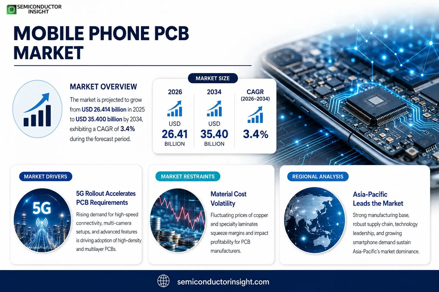
Mobile Phone PCB market size was valued at USD 26.414 billion in 2025; it is projected to reach USD 35.400 billion by 2034, reflecting an implied CAGR of approximately 3.4% over the forecast horizon.
Mobile phone printed circuit boards (Mobile Phone PCBs) are core components that provide electrical interconnection, signal transmission,and functional integration within smartphones.The portfolio includes rigid PCBs,the high‑density interconnect (HDI) PCBs,flexible PCBs (FPCs),and rigid‑flex PCBs,and they are used across main logic boards,Rf modules,camera modules,and display/battery connections.The sector’s expansion is underpinned by continuous upgrades in smartphone technologysuch as higher‑speed connectivity,multi‑camera architectures,and thinner form factorsthat raise demands for higher routing densityand signal integrity;however,the volatility of raw‑material costsand substantial capital requirementsfor advanced manufacturing pose notable challengesfor new entrants.
MARKET DRIVERS
5G Rollout Accelerates PCB Requirements
The deployment of 5G networks compels manufacturers to embed higher‑frequency components, which in turn drives the adoption of finer line‑width PCBs. Mobile Phone PCB Market players that can supply multilayer stacks with tighter tolerances are gaining a competitive edge, as carriers demand devices capable of sustaining peak data rates beyond 3 Gbps.
Push for Ultra‑Thin Form Factors
Consumers now expect smartphones to be slimmer yet more powerful. This trend forces designers to reduce board thickness while maintaining signal integrity, prompting a shift toward high‑density interconnect (HDI) solutions. Mobile Phone PCB Market firms that have invested in laser‑drilled micro‑vias report yield improvements of up to 12 %.
➤ “Design teams that master HDI and advanced substrate technologies can command premium pricing and secure long‑term contracts with flagship OEMs.”
Meanwhile, the surge in camera megapixel counts forces PCB layouts to accommodate larger sensor arrays and complex lens modules. Engineers are turning to rigid‑flex hybrids, a move that opens a niche worth an estimated $85 million in 2024, while also demanding tighter coordination across supply chains.
MARKET CHALLENGES
Material Cost Volatility
Raw‑material prices for copper and specialty laminates have swung 15 % year‑over‑year, squeezing margins for manufacturers that lack hedging strategies. Companies that rely on spot purchases see profitability erode, prompting a reevaluation of cost‑pass‑through mechanisms.
Other Challenges
Supply‑Chain Bottlenecks
The lingering effects of pandemic‑related disruptions still manifest as lead‑time extensions for high‑frequency components. OEMs are increasingly demanding localized production, which raises capital expenditures for new fab sites.
MARKET RESTRAINTS
Stringent Environmental Regulations
Regulatory bodies across Europe and Asia have tightened limits on halogenated flame retardants, forcing PCB suppliers to qualify alternative chemistries. The certification process can add six to nine months to product launch cycles, discouraging smaller players.In addition, the rise of electronic waste (e‑waste) legislation imposes higher recycling fees. Manufacturers that cannot demonstrate closed‑loop material recovery face penalties that directly affect the bottom line.Trade tensions between major economies also create uncertainty around tariff structures. Companies that depend on cross‑border component imports must navigate fluctuating duties, which can quickly render previously profitable designs unviable.
MARKET OPPORTUNITIES
Flexible and Stretchable PCBs
Emerging form factorssuch as foldable phones and wearable devicesrequire substrates that bend without compromising performance. Early adopters of polyimide‑based flexible PCBs are projected to capture a share of the segment that could exceed $120 million by 2026.
Integration of Antenna‑in‑Package (AiP) Solutions
Embedding antennas directly onto the PCB reduces module count and frees up interior space. Firms that can reliably integrate AiP across mmWave bands stand to benefit from the premium‑segment devices that command higher unit prices.Finally, the convergence of smartphones with IoT functionality opens a pathway for multi‑function boards that support both communication and sensor interfacing. This cross‑application potential creates a runway for revenue diversification beyond traditional handset cycles.
Mobile Phone PCB Market Trends
Shift Toward High‑Density HDI and Flexible Designs
The proliferation of 5G radios, multi‑camera arrays, and under‑display sensors forces manufacturers to pack more signal paths into ever‑smaller footprints. Consequently, Mobile Phone PCB Market is seeing a decisive move from conventional rigid boards to high‑density interconnect (HDI) structures, multi‑layer flexible circuits, and rigid‑flex hybrids. These formats deliver tighter trace spacing, superior impedance control, and the ability to bend around cramped chassis sections. Suppliers that have invested in finer photo‑image technology and advanced lamination processes are capturing the premium margin pool, while lower‑cost producers face pricing pressure as volume growth flattens. The net effect is a reallocation of revenue toward value‑added offerings rather than sheer unit count.
Other Trends
Supply‑Chain Consolidation and Margin Pressure
As design cycles shorten and OEMs demand tighter tolerances, the ecosystem around Mobile Phone PCB Market is consolidating around a handful of manufacturers with proven high‑mix capabilities. These players leverage long‑term engineering collaborations to guarantee yield consistency, which in turn secures the gross‑margin band of 15 %‑20 % reported across the sector. Smaller entrants find it increasingly difficult to meet the capital outlay for next‑generation equipment, leading to a gradual exit from the low‑end segment. For OEMs, the trade‑off is clearer: strong supplier lock‑in delivers reliability, but it also reduces bargaining leverage in price negotiations.
Emerging Materials and Multi‑Layer Integration
Parallel to structural changes, material innovation is reshaping board performance. Polyimide substrates, prized for thermal stability, are gaining ground in flagship devices where heat dissipation from high‑power SoCs is critical. At the same time, the adoption of multi‑material stackscombining FR‑4, glass‑fiber, and ceramic layersenables designers to tailor dielectric properties for assorted RF and high‑speed digital blocks. This trend nudges Mobile Phone PCB Market toward a more differentiated product mix, where expertise in material science becomes a competitive moat. Companies that can orchestrate cross‑disciplinary design teams are better positioned to offer turnkey solutions that align with OEM roadmaps, turning technical complexity into a strategic advantage.
COMPETITIVE LANDSCAPE
Key Industry Players
Mobile Phone PCB Competitive Overview – 2025 Snapshot
The upper tier of the mobile‑phone PCB supply chain is dominated by a handful of manufacturers that have translated deep process expertise into premium HDI and high‑layer‑count flexible products. Zhen Ding Technology and Unimicron Technology command a sizable share of the advanced‑HDI segment, leveraging multi‑year collaborations with leading smartphone OEMs to secure design‑in status for flagship devices. Ibiden and AT&S complement this core by pairing high‑volume capacity with robust yield‑control systems, allowing them to serve both flagship and upper‑mid‑range programs while preserving gross margins above the industry average. Their ability to integrate material science advancessuch as low‑CTE polyimide and high‑frequency copper foilcreates a barrier for new entrants and reinforces a market structure where scale, reliability, and long‑term engineering partnerships drive competitive advantage.Beyond the tier‑one group, a diverse set of regional and specialist firms occupies the middle and low‑end niches, each carving out value through cost efficiency or technology focus. Tripod Technology and Shennan Circuits Company have built reputations in high‑volume rigid‑flex production, supplying OEMs that prioritize compact module integration for foldable and ultra‑thin devices. Companies such as Kinwong, Victory Giant Technology, and Jiangxi Redboard Technology concentrate on flexible PCB platforms, often winning contracts for camera and sensor interconnects where routing density is paramount. Smaller players like Suntak Technology, Bomin Electronics, and Huizhou CEE Technology operate with agile manufacturing footprints, enabling rapid response to short sprint cycles but exposing them to pricing pressure from larger rivals. The overall picture is one of consolidation pressure, where strategic alliances or capacity upgrades are likely pathways for niche firms aiming to climb the value chain.
List of Key Mobile Phone PCB Companies Profiled
- Zhen Ding Technology
- Unimicron Technology
- Compeq
- Nippon Mektron
- Ibiden
- AT&S
- Samsung Electro-Mechanics
- TTM Technologies
- Tripod Technology
- DSBJ
- Shennan Circuits Company
- Kinwong
- Zhuhai Founder
- Interflex
- Victory Giant Technology
- Jiangxi Redboard Technology
- Suntak Technology
- Bomin Electronics
- Huizhou CEE Technology
Segment Analysis:
| Segment Category | Sub-Segments | Key Insights |
| By Type |
|
HDI PCB
|
| By Application |
|
Flagship Smartphone
|
| By End User |
|
Smartphone OEMs
|
| By Material |
|
Polyimide
|
| By Process Complexity |
|
High‑Density Blind/Buried Vias
|
Regional Analysis: Mobile Phone PCB Market
Asia-Pacific
A dense network of tier‑1 and tier‑2 suppliers clusters around major manufacturing hubs, allowing rapid substitution of components when demand spikes. This concentration reduces lead times and gives regional firms an edge in cost management.
Local research institutes prioritize low‑dielectric laminates and high‑frequency prepregs, enabling thinner, lighter PCBs that meet emerging form‑factor trends without compromising signal integrity.
Harmonized environmental and safety standards across the sub‑region simplify certification pathways, allowing manufacturers to scale new designs across multiple markets with minimal rework.
Engineering programs in Singapore, Taiwan, and India feed a steady stream of specialists versed in high‑density interconnect technology, sustaining the region’s capacity for complex multilayer board production.
North America
North America remains a critical testing ground for premium Mobile Phone PCB innovations, where flagship devices demand the highest reliability levels. Companies here emphasize stringent validation protocols and invest heavily in traceability software, aligning production with the rigorous standards of major carriers. While cost pressures push some OEMs to source components from lower‑cost regions, domestic firms retain a niche by offering rapid prototyping services and short‑run capabilities that support niche market entrants and early‑stage product launches. The strategic focus on cybersecurity and supply‑chain resilience also shapes investment decisions, encouraging manufacturers to adopt advanced inspection techniques and secure material sourcing.
Europe
In Europe, Mobile Phone PCB Market is characterized by a strong orientation toward sustainable manufacturing practices and regulatory compliance. Manufacturers respond to stringent RoHS and REACH directives by integrating greener laminates and exploring recyclable substrate options. Premium brand presence drives a demand for high‑frequency boards that support emerging 5G bands, prompting European firms to specialize in precision etching and fine‑line routing. Collaboration between automotive and mobile sectors has introduced cross‑industry knowledge transfer, especially in robust design for harsh environments, offering a competitive advantage in rugged device segments.
South America
South American markets exhibit a gradual shift from legacy board architectures toward more compact, multilayer designs, reflecting rising consumer expectations for flagship‑grade features. Local assemblers focus on cost‑effective production methods, leveraging governmental incentives aimed at boosting electronics manufacturing. The region’s growing middle class fuels demand for mid‑range smartphones, compelling PCB suppliers to balance quality with price sensitivity. Partnerships with Asian manufacturers enable knowledge transfer, gradually raising the technical baseline and opening avenues for regional firms to capture niche export opportunities.
Middle East & Africa
The Middle East & Africa segment presents a heterogeneous landscape where affluent Gulf markets drive demand for ultra‑premium devices, while Sub‑Saharan economies prioritize affordability. PCB providers adapt by offering modular design kits that can be customized for varying performance tiers. Investment in smart‑city infrastructure introduces ancillary demand for high‑speed connectivity boards, indirectly influencing mobile PCB specifications. Moreover, regional trade agreements are facilitating cross‑border component flows, allowing local manufacturers to scale up operations without substantial capital outlays, thereby enhancing their role in the broader Mobile Phone PCB ecosystem.
Report Scope
This market research report provides a comprehensive analysis of the Mobile Phone PCB Market , covering the forecast period 2026–2034. It offers detailed insights into market dynamics, technological advancements, competitive landscape, and key trends shaping the industry.
Key focus areas of the report include:
- Market Overview: The report begins with an overview outlining its current market scenario, key growth indicators, and industry transformation drivers. It discusses macroeconomic factors, demand–supply balance, regulatory landscape, and the strategic role of semiconductors in powering advancements across industries such as automotive, telecommunications, consumer electronics, and industrial automation.
- Market Size & Forecast: Historical data and future projections for revenue, unit shipments, and market value across major regions and segments.
- Segmentation Analysis: Detailed breakdown by product type, technology, application, and end-user industry to identify high-growth segments and investment opportunities.
- Regional Insights: Insights into market performance across North America, Europe, Asia-Pacific, Latin America, and the Middle East & Africa, including country-level analysis where relevant.
- Competitive Landscape: Profiles of leading market participants, including their product offerings, R&D focus, manufacturing capacity, pricing strategies, and recent developments such as mergers, acquisitions, and partnerships.
- Technology Trends & Innovation: Assessment of emerging technologies, integration of AI/IoT, semiconductor design trends, fabrication techniques, and evolving industry standards.
- Market Drivers & Restraints: Evaluation of factors driving market growth along with challenges, supply chain constraints, regulatory issues, and market-entry barriers.
- Stakeholder Insights: Insights for component suppliers, OEMs, system integrators, investors, and policymakers regarding the evolving ecosystem and strategic opportunities.
Primary and secondary research methods are employed, including interviews with industry experts, data from verified sources, and real-time market intelligence to ensure the accuracy and reliability of the insights presented.
FREQUENTLY ASKED QUESTIONS:
What is the current market size of Mobile Phone PCB Market?
-> Mobile Phone PCB Market was valued at USD 26,414 million in 2025 and is expected to reach USD 33,314 million by 2032.
Which key companies operate in Mobile Phone PCB Market?
-> Key players include Zhen Ding Technology, Unimicron Technology, Compeq, Nippon Mektron, Ibiden, AT&S, Samsung Electro-Mechanics, TTM Technologies, Tripod Technology, DSBJ, Shennan Circuits Company, Kinwong, Zhuhai Founder, Interflex, Victory Giant Technology, Jiangxi Redboard Technology, Suntak Technology, Bomin Electronics, Huizhou CEE Technology.
What are the key growth drivers?
-> Key growth drivers include 5G connectivity, high‑performance SoCs, multi‑camera architectures, thinner and more integrated device designs, and ongoing smartphone miniaturization.
Which region dominates the market?
-> Asia remains the dominant region, driven by large smartphone OEM bases in China, South Korea, Japan, and expanding markets in Southeast Asia and India.
What are the emerging trends?
-> Emerging trends include higher‑layer HDI designs, increased adoption of flexible and rigid‑flex PCBs, multi‑material solutions, and tighter integration of PCB functionality with system modules.
Get Sample Report PDF for Exclusive Insights
Report Sample Includes
- Table of Contents
- List of Tables & Figures
- Charts, Research Methodology, and more...
 Download Sample Report PDF







