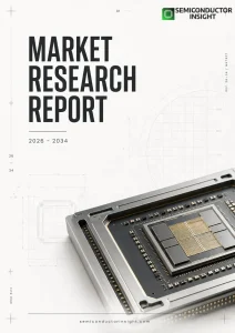
SELECTED REPORT
Semiconductor Process Equipment (SPE) Market Size, Share & Industry Analysis, By Type (Etching Equipment, Deposition/Thin Film Equipment, Inspection & Metrology, Coater & Developer, Lithography, Cleaning, Ion Implantation, CMP, Heat Treatment), By Application (Foundry & Logic, NAND, DRAM, Silicon Wafer Manufacturing, Test, Assembly & Packaging), By Wafer Size (200mm & Below, 300mm), By End User (Foundries, IDMs, Memory Manufacturers, OSATs), and Regional Forecast, 2026-2034
Semiconductor Equipment

Semiconductor Process Equipment (SPE) Market Size, Share & Industry Analysis, By Type (Etching Equipment, Deposition/Thin Film Equipment, Inspection & Metrology, Coater & Developer, Lithography, Cleaning, Ion Implantation, CMP, Heat Treatment), By Application (Foundry & Logic, NAND, DRAM, Silicon Wafer Manufacturing, Test, Assembly & Packaging), By Wafer Size (200mm & Below, 300mm), By End User (Foundries, IDMs, Memory Manufacturers, OSATs), and Regional Forecast, 2026-2034

Semiconductor process equipment (spe) market was valued at USD 105.48 billion in 2025, is estimated at USD 112.72 billion in 2026, and is projected to reach USD 191.75 billion by 2034, advancing at a 6.9%...

REPORT TYPE Market Research
DELIVERY Digital
View Full Report →

What you'll receive

✓
Report Scope

Understand the markets, technologies and applications covered.

✓
Table of Contents

Review the report structure and detailed research coverage.

✓
Sample Analysis

Evaluate the depth and style of the market intelligence.

✓
Analyst Assistance

Discuss specific questions or custom research requirements.

↓
REQUEST SAMPLE

Download a complimentary sample

Complete the form and our research team will send you a sample of:

Semiconductor Process Equipment (SPE) Market Size, Share & Industry Analysis, By Type (Etching Equipment, Deposition/Thin Film Equipment, Inspection & Metrology, Coater & Developer, Lithography, Cleaning, Ion Implantation, CMP, Heat Treatment), By Application (Foundry & Logic, NAND, DRAM, Silicon Wafer Manufacturing, Test, Assembly & Packaging), By Wafer Size (200mm & Below, 300mm), By End User (Foundries, IDMs, Memory Manufacturers, OSATs), and Regional Forecast, 2026-2034
🔒

Your information is used only to respond to your research request.

Market Intelligence Detailed market sizing and forecasts
Technology Analysis Semiconductor technology and application intelligence
Competitive Research Company and ecosystem analysis
Analyst Support Assistance for specific research needs