The Role of Micro Drilling Technology in Semiconductor Packaging
Micro Drilling Technology Overview
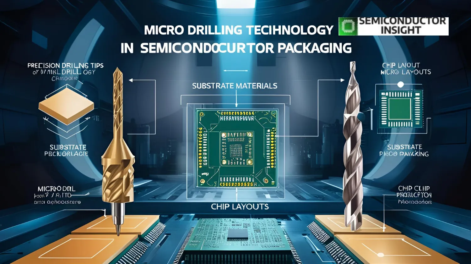
As electronic devices become smaller and more powerful, the demand for advanced packaging technologies in the semiconductor industry continues to rise. At the core of this evolution is micro drilling technology, a precision process that plays a critical role in fabricating high-density interconnect (HDI) structures. Micro drilling enables the creation of microscopic vias and holes essential for routing connections between various layers in integrated circuit (IC) substrates.
Micro drilling, often performed using laser or mechanical methods, is vital for forming fine patterns and through-holes that support multilayer printed circuit boards (PCBs). These components serve as the foundational platforms for mounting and interconnecting semiconductor devices in compact and complex electronic assemblies. As semiconductor packaging trends move toward miniaturization, increased performance, and cost efficiency, micro drilling technology has become indispensable.
How Micro Drilling Supports Semiconductor Packaging
High-Density Interconnect (HDI) Structures
Micro drilling is used to create microvias, which are tiny holes that enable vertical electrical connections between layers in HDI PCBs. These structures are critical in modern packaging methods such as system-in-package (SiP) and chip-scale packages (CSPs), where space optimization is a priority.
Laser and Mechanical Drilling Methods
There are two primary micro drilling techniques used in semiconductor packaging:
- Laser Drilling: Employs UV or CO2 lasers to create precise, clean microvias in substrates like polyimide or FR-4. It is ideal for small diameters (under 100 microns) and high-speed production.
- Mechanical Drilling: Involves the use of ultra-fine drills and spindles to bore holes in rigid substrates. This method provides high accuracy and is typically used in multilayer board production.
Via Formation and Through-Hole Interconnects
Micro drilling enables through-hole and blind/buried via formation, which facilitates high-speed signal transmission and reliable power delivery across layers. These interconnects reduce parasitic inductance and improve thermal performance.
Enabling Fine-Pitch Designs
Advanced semiconductor devices often require ultra-fine pitch configurations. Micro drilling supports these layouts by enabling extremely small hole sizes and tight tolerances, allowing for higher I/O counts without increasing the package footprint.
Enhanced Thermal and Electrical Performance
By enabling more efficient routing and interconnects, micro drilling contributes to better thermal management and electrical conductivity. This leads to improved device reliability and longer operational life.
Micro Drilling Technology Future Growth Opportunities
The micro drilling market is set to expand significantly in response to the rapid development of 5G, IoT, automotive electronics, and AI chips. The following areas present major opportunities:
- Increasing adoption of HDI and advanced substrate technologies in mobile and wearable electronics.
- Growth of heterogeneous integration, requiring denser packaging and more complex via structures.
- Rising demand for IC substrates in high-performance computing and data center applications.
- Development of new materials (e.g., BT resin, ABF substrate) that require customized drilling techniques.
- Investment in next-gen laser drilling systems for enhanced precision and throughput.
The global micro drilling machine market is projected to grow at a CAGR of over 6% from 2023 to 2030, driven by the semiconductor industry’s scaling and packaging needs.
Conclusion
Micro drilling technology is a cornerstone of advanced semiconductor packaging. It enables the miniaturization and functional density required by modern electronic systems. As the industry shifts toward more compact and powerful devices, micro drilling will continue to support the critical transitions in substrate design and manufacturing.
FAQs
Q: What is micro drilling in semiconductor packaging?
A: Micro drilling is the precision creation of small-diameter holes or vias in PCBs or substrates to form electrical interconnects.
Q: How does micro drilling support HDI PCB manufacturing?
A: It enables the formation of microvias and through-holes for vertical connections between layers, supporting compact circuit designs.
Q: What materials are typically used in micro drilling?
A: Common materials include FR-4, polyimide, BT resin, and ABF substrates, often used in multilayer boards and IC substrates.
Q: What are the benefits of laser drilling over mechanical drilling?
A: Laser drilling offers higher precision, faster production speeds, and is ideal for small hole diameters and complex patterns.
Q: Which industries drive the demand for micro drilling in semiconductors?
A: Consumer electronics, automotive, telecommunications, and data centers are major drivers due to the need for advanced packaging.
Shubham K
Shubham is a seasoned market researcher specializing in the semiconductor industry, providing in-depth analysis on emerging trends, technological advancements, and market dynamics. With extensive experience in semiconductor manufacturing, supply chain analysis, and competitive intelligence, Shubham delivers actionable insights that help businesses navigate the evolving landscape of chip design, fabrication, and applications. His expertise spans key areas such as AI-driven semiconductors, advanced packaging, memory technologies, and foundry trends.At SemiconductorInsight, Shubham combines data-driven research with strategic foresight, offering thought leadership that empowers industry professionals, investors, and technology innovators to make informed decisions.
Comments (0)