

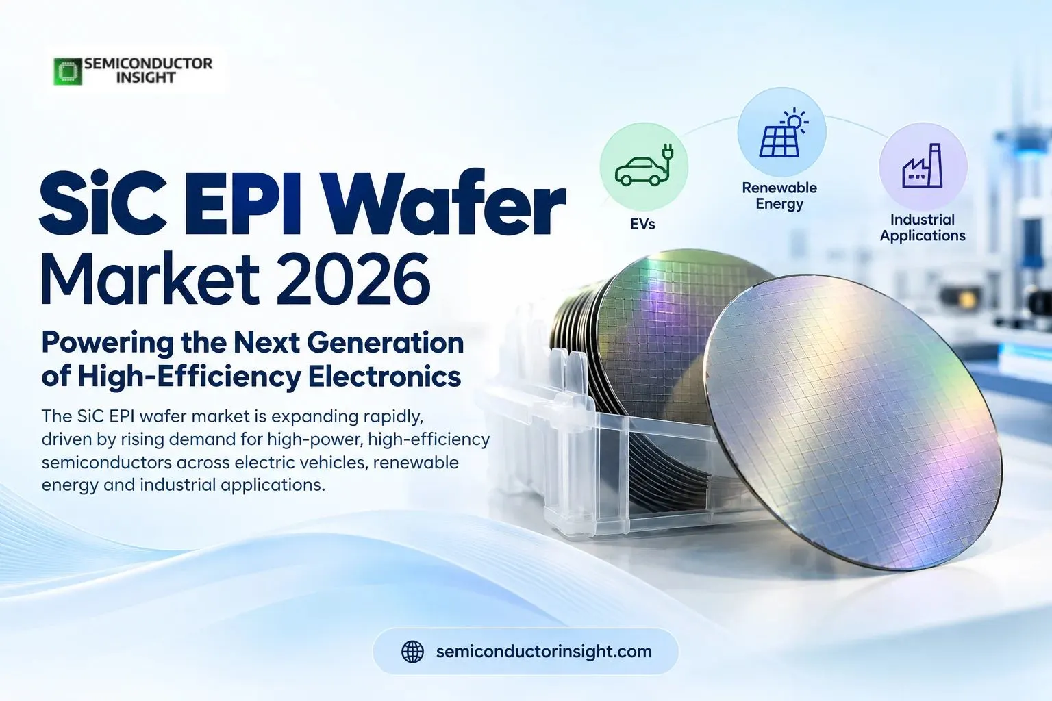
SiC EPI Wafer Market 2026 and the Shift toward 200 mm Power Semiconductor Manufacturing
Silicon carbide epitaxial wafers are becoming increasingly important as semiconductor manufacturers develop power devices capable of handling higher voltages, temperatures, and switching frequencies. An epitaxial wafer consists of a silicon carbide substrate covered with a precisely grown crystalline layer that determines key electrical characteristics of the finished device.
Demand extends beyond electric vehicles into fast-charging equipment, renewable energy converters, industrial drives, rail systems, and high-power data-center infrastructure. In April 2026, Coherent announced advances in thick SiC epitaxy for power devices rated up to 10 kV, targeting applications including AI data centers and industrial power systems.
Why 200 mm Wafer Production Is Changing the Manufacturing Equation?
Larger wafers can accommodate more individual semiconductor dies, potentially reducing manufacturing costs per device when yields and equipment utilization remain competitive. Moving from 150 mm to 200 mm, however, requires consistent epitaxial thickness, doping uniformity, and defect control across a larger surface.
In September 2025, Wolfspeed commercially launched its 200 mm SiC materials portfolio and made 200 mm epitaxial wafers available for customer qualification. This marked a significant step toward scaling production beyond traditional wafer formats.
North America and the Expansion of SiC Materials Capacity
- The United States has an established SiC materials ecosystem, supported by wafer producers, power semiconductor manufacturers, and investments in domestic production.
- Wolfspeed’s John Palmour Manufacturing Center in North Carolina is designed to increase materials capacity substantially, with a stated target of creating 1,800 jobs by 2035.
- Coherent is another important US-based supplier, offering epitaxial wafers in diameters up to 200 mm.
- Its April 2026 announcement on thick epitaxy for devices up to 10 kV highlights how material engineering is expanding into high-voltage industrial and data-center applications.
Europe and the Move toward Integrated Wafer Production
Germany, Austria, France, and Italy form important parts of Europe’s SiC semiconductor ecosystem. Infineon began releasing products manufactured using 200 mm SiC technology in Villach, Austria, in 2025, while its Malaysian facility is also transitioning toward the larger wafer format.
Italy is developing an integrated SiC campus covering substrate development, epitaxial growth, wafer fabrication, and packaging. STMicroelectronics announced a planned investment of approximately €5 billion, with a target capacity of up to 15,000 wafers per week at full build-out by 2033.
Asia-Pacific and the Strength of Cross-Border Manufacturing
Japan, China, South Korea, and Malaysia are relevant to the regional SiC ecosystem through semiconductor manufacturing, materials development, electronics production, and automotive supply chains.
Malaysia is especially notable for its role in Infineon’s 200 mm SiC manufacturing plans at Kulim. Japan’s DENSO and Mitsubishi Electric have also committed a combined $1 billion investment in Coherent’s SiC business, alongside long-term supply arrangements for SiC substrates and epitaxial wafers.
These developments illustrate how wafer materials, device manufacturing, and automotive demand are increasingly linked across national supply chains.
Don’t Forget to Surf Our Updated Report for More Detailed Analysis: https://semiconductorinsight.com/report/sic-epi-wafer-market/
Latin America and the Growth of Downstream Power Electronics
Brazil and Mexico offer relevant opportunities through automotive manufacturing, industrial electrification, renewable energy installations, and power conversion equipment. These applications can create demand for SiC-based devices even where local epitaxial wafer production remains limited.
Brazil’s renewable energy and electric mobility projects provide potential downstream markets for inverters, charging systems, and industrial power electronics. Mexico’s automotive manufacturing base creates another route for SiC adoption through vehicle power systems and electronics supply chains. The region’s opportunity is therefore better understood through device demand and supply-chain integration than through claims of established wafer-production leadership.
Middle East and Africa and the Emerging Power Infrastructure Opportunity
- Saudi Arabia, the United Arab Emirates, and South Africa are relevant to downstream SiC applications through grid modernization, renewable energy, industrial power conversion, and electric mobility infrastructure.
- SiC power devices can help improve conversion efficiency in solar inverters, high-power charging systems, and industrial equipment.
- However, these applications do not automatically translate into local epitaxial wafer manufacturing.
- Regional progress will depend on electronics supply-chain investment, technical partnerships, and the development of downstream semiconductor capabilities.
What Buyers Will Examine Beyond Wafer Diameter?
Wafer qualification depends on more than size. Buyers evaluate defect density, epitaxial thickness, doping uniformity, wafer bow, yield consistency, and supplier reliability. As 200 mm production expands, manufacturers that demonstrate repeatable material quality and support demanding high-voltage device designs will be well positioned to serve the next generation of power electronics.

Comments (0)