PPLN Chip Industry Surges with U.S. Foundry Launch and Academic Breakthroughs: Market to Hit $214 Million by 2032
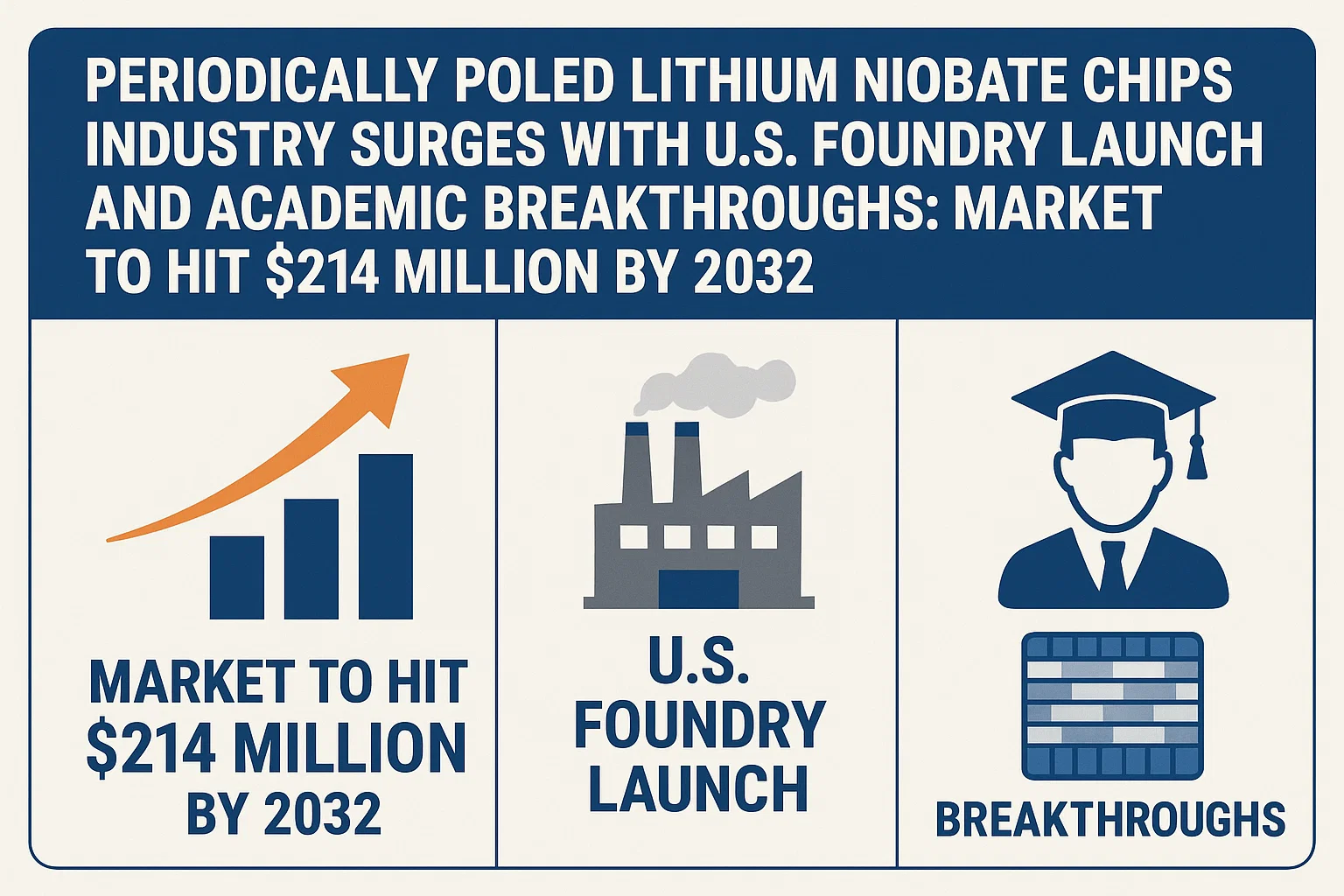
In the ever-evolving landscape of integrated photonics and quantum technologies, few materials have garnered as much attention in recent years as Periodically Poled Lithium Niobate (PPLN). These chips are revolutionizing the way light is manipulated on-chip, with remarkable applications across telecommunications, quantum computing, sensing, and nonlinear optics. As of 2024, the PPLN chips market was valued at US$ 127 million and is projected to surge to US$ 214 million by 2032, exhibiting a compound annual growth rate (CAGR) of 7.8% between 2025 and 2032.
This blog dives deep into the recent developments, academic breakthroughs, industrial investments, and market drivers shaping the future of PPLN chips. We’ll explore how pioneering fabrication techniques and the expansion of domestic foundries are turning this advanced photonic material into a critical enabler for next-generation technologies.
1. Understanding Periodically Poled Lithium Niobate (PPLN)
Lithium niobate (LiNbO3) is a crystalline material known for its outstanding electro-optic, acousto-optic, and nonlinear optical properties. Periodic poling is a fabrication technique that reverses the crystal’s ferroelectric domains at regular intervals, enabling quasi-phase matching (QPM). This process greatly enhances nonlinear interactions such as second harmonic generation (SHG), sum-frequency generation (SFG), and optical parametric oscillation (OPO), making PPLN a core component in frequency conversion and quantum photonic circuits.
With the advent of thin-film lithium niobate (TFLN), researchers and companies have managed to miniaturize high-performance devices while maintaining or even improving optical efficiencies. The result is a dramatic improvement in size, speed, and integration capabilities compared to traditional bulk optics.
2. Market Overview and Forecast (2025–2032)
The global market for PPLN chips has experienced robust growth in recent years due to increasing demand from quantum information systems, high-speed telecommunications, LiDAR sensors, and integrated photonic platforms.
- 2024 Market Size: US$ 127 million
- 2032 Projected Size: US$ 214 million
- Forecast Period CAGR (2025-2032): 7.8%
Key Market Drivers:
- Rising investment in quantum computing and secure communications
- Expansion of 5G/6G optical infrastructure
- Emergence of photonic integrated circuits (PICs)
- Government and institutional funding for domestic photonics manufacturing
Key Restraints:
- High fabrication costs and precision requirements
- Limited foundry access until recently
- Complex packaging and integration for commercial-scale products
3. Groundbreaking Industry Developments (2024–2025)
a. Quantum Computing Inc. Launches U.S.-Based TFLN Foundry
In May 2025, Quantum Computing Inc. (QCi) inaugurated a fully operational TFLN chip fabrication facility at Arizona State University’s Research Park. This strategic move not only boosts the North American supply chain for lithium niobate chips but also supports scalable production of periodically poled devices.
The Arizona fab, completed in early 2025, is equipped for commercial-scale output of photonic integrated circuits and periodically poled structures. QCi’s fab has been instrumental in fulfilling the rising demand for telecom, datacom, quantum computing, and optical sensing applications.
This development reflects a broader movement towards reshoring high-tech semiconductor and photonic manufacturing capabilities in the U.S., enhancing both innovation speed and supply chain resilience.
b. Surge in Pilot Orders Validates Industry Demand
- January 2025: QCi reported its third and fourth major customer orders. One came from a leading European technical university focusing on quantum optics, while the other was from a Canadian photonic design startup developing PICs for advanced sensing.
- January 30, 2025: The fifth order was confirmed from a Canadian quantum photonics lab. These orders highlight real-world adoption of PPLN-based solutions for photon-pair generation, SHG, and parametric down-conversion systems.
These rapid commercial engagements validate the scalability and practical value of PPLN chips in research and enterprise-grade systems.
c. Open Access to Process Design Kit (PDK)
To foster faster adoption of lithium niobate technologies, QCi also released an open-source Photonic PDK through the GDSFactory ecosystem. This empowers engineers and designers to rapidly prototype and validate PPLN-based devices on standard platforms, lowering entry barriers and expediting innovation cycles.
4. Academic and Research Breakthroughs
a. High-Efficiency PPLN Waveguide Fabrication (April 2025)
A 2025 academic study detailed a novel fabrication method for creating ultra-low-loss, high-conversion PPLN waveguides using chemo-mechanical polishing and high-voltage poling. Key metrics:
- Surface smoothness approaching atomic precision
- Propagation losses as low as 0.25–1 dB/cm
- SHG efficiencies around 750%/W
This opens doors for more efficient frequency-doubling and entangled photon-pair generation, essential for quantum light sources and telecom wavelength conversion.
b. Layer-Poled Lithium Niobate Devices (October 2024)
Another significant advancement came from researchers working on Layer-Poled Lithium Niobate (LPLN). These devices exhibited extraordinary nonlinear properties:
- SHG efficiency: 4615% W⁻¹cm⁻²
- On-chip photon-pair brightness: 3.1 × 10⁶ Hz·nm⁻¹·mW⁻²
Such metrics make LPLN structures ideal for high-performance quantum photonics, nonlinear signal processing, and metrology applications.
5. Strategic Implications and Industry Impact
a. Quantum Photonics and Secure Communication
PPLN chips are poised to become foundational elements in future quantum communication networks. Their ability to efficiently manipulate and entangle photons allows for secure key distribution (QKD) and quantum repeater functionality. With governments investing heavily in post-quantum cryptography, this domain will remain a central growth vector for the PPLN market.
b. Telecom and 6G Infrastructure
As the world edges towards 6G networks, PPLN chips will be instrumental in achieving ultra-high-speed data transfer through wavelength conversion and optical switching. Their compact footprint and high conversion efficiencies make them ideal for dense wavelength-division multiplexing (DWDM) systems.
c. Photonic Integration
With platforms like silicon photonics and indium phosphide dominating integration, lithium niobate-on-insulator (LNOI) provides a powerful hybrid alternative. It supports:
- Compact footprint
- High optical confinement
- CMOS-compatible processing
Combined with periodic poling, this enhances device versatility for all-optical computing and AI accelerators.
6. Challenges Ahead
Despite rapid advancements, certain hurdles persist:
- Yield Issues: Achieving uniform periodic poling on thin films remains technically challenging.
- Thermal Instability: Some applications demand extreme temperature resilience, which lithium niobate alone doesn’t always offer.
- Design Complexity: Integration with other photonic platforms and thermal-optic tunability can be limiting factors.
Collaborative research and development, along with standardization efforts, will be key to overcoming these obstacles.
7. Competitive Landscape
Several startups and photonics giants are vying for leadership in the PPLN market:
- Quantum Computing Inc.: U.S.-based pioneer with a commercial TFLN fab
- Ligentec: Specializing in high-confinement LNOI platforms
- HyperLight Corp.: Focused on ultrafast lithium niobate modulators
- CSEM (Switzerland) and IMEC (Belgium): European R&D centers contributing to PPLN innovation
As ecosystem maturity grows, more vertical and horizontal collaborations are expected.
8. A Bright Path Ahead
The resurgence of interest in periodically poled lithium niobate is more than a research renaissance—it is a commercial and technological tipping point. With domestic fabs now operational, academic methods reaching industrial feasibility, and quantum/telecom markets hungry for performance breakthroughs, PPLN chips are set to become foundational in the photonics era.
As the market heads toward a valuation of US$ 214 million by 2032, the convergence of high-precision engineering, scalable manufacturing, and real-world demand will cement PPLN’s role in powering the next decade of photonic innovation.
Comments (0)