New Torque Clustering Method Promises Auto‑Adaptive, Parameter‑Free AI for Large Datasets
In today’s fast-evolving semiconductor and advanced electronics manufacturing landscape, one segment has been steadily gaining prominence—Cluster Tools. Originally developed to streamline semiconductor wafer fabrication, cluster tools have now expanded their footprint across multiple industries including photovoltaics, MEMS, LED, and data storage devices. As of 2024, the global Cluster Tools market stands tall at USD 4.73 billion, and projections indicate a surge to USD 8.94 billion by 2032, reflecting a CAGR of 9.5% from 2025 to 2032.
Access Your Free Sample Report- Cluster Tools Market
What Are Cluster Tools?
Cluster tools are integrated systems used in semiconductor manufacturing to carry out multiple processing steps (etching, deposition, cleaning, etc.) under vacuum in a single platform. These tools consist of a central transfer chamber surrounded by various process modules (PMs) and load lock chambers. The key advantage is increased yield, reduced contamination, and high throughput, making them vital in nanometer-scale fabrication.
With the explosive demand for chips in AI, automotive electronics, 5G, and edge computing, the efficiency and modularity of cluster tools have never been more relevant.
Market Dynamics: What’s Driving the Surge?
Shift Toward Modular and Flexible Fabrication
Today’s chipmakers seek greater agility. Traditional batch tools can’t keep up with the demand for smaller geometries, multi-patterning, and new materials. Cluster tools—being highly configurable—allow fabs to integrate custom recipes, swap modules, and adapt to diverse wafer sizes and process technologies. This flexibility is pushing adoption in both leading-edge and legacy node production.
Explosive Growth in Electric Vehicles and AI Chips
The global pivot to electric mobility and data-driven services is increasing the demand for advanced logic and memory chips. Cluster tools are particularly well-suited to handle 3D NAND, FinFET, and gate-all-around (GAA) structures due to their controlled environment and modular capabilities. They’re being deployed in next-gen fabs manufacturing AI accelerators, edge inference processors, and advanced sensors for EVs.
Rise of Fabless Manufacturing and Foundry Ecosystems
As more companies embrace fabless models, reliance on pure-play foundries like TSMC, GlobalFoundries, and UMC is growing. These foundries are expanding capacity, modernizing with 300mm cluster platforms, and investing in automation and wafer-level packaging—all domains where cluster tools are indispensable.
Recent Developments and Industry Trends
Let’s explore key news and events in the cluster tools ecosystem, drawn from recent developments across leading players and top tech sources:
- AI-Driven Process Optimization in Cluster Platforms
One of the biggest leaps in recent years is the integration of AI and ML into cluster tool systems. Semiconductor equipment companies are embedding predictive analytics into their platforms to optimize chamber conditions, detect anomalies, and reduce cycle time.
🔍 Example: Companies like Applied Materials and Lam Research have introduced AI software layers that interface with cluster tools to optimize vacuum pressures, temperature gradients, and plasma uniformity in real time.
“By embedding AI into our toolsets, we’ve seen 15–20% improvements in wafer throughput and reduced downtime by over 30%.” – CTO, Leading Semi Tool OEM
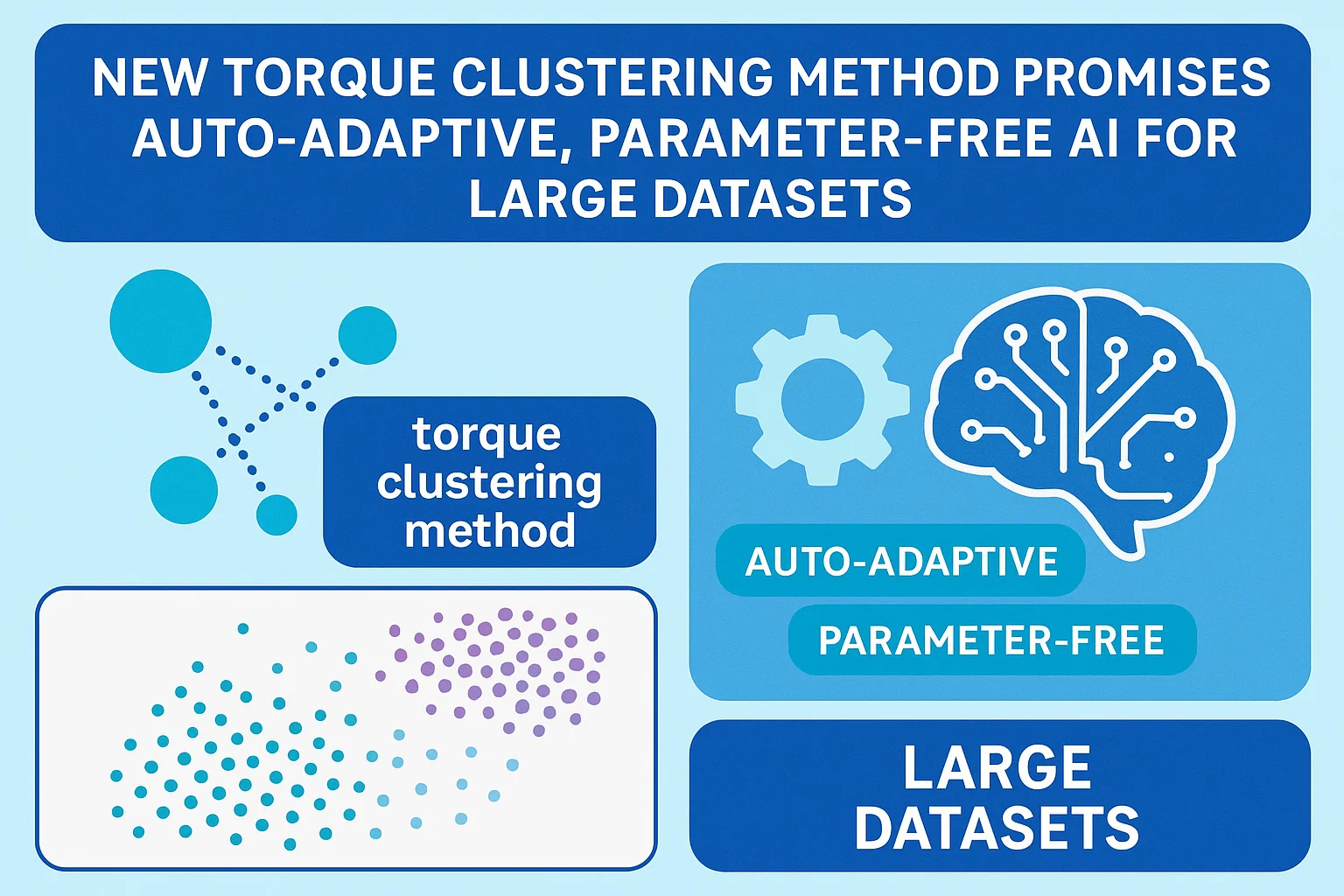
- Torque Clustering Algorithm: Breakthrough in Process Analysis
In early 2025, the University of Technology Sydney unveiled a revolutionary method called Torque Clustering, which autonomously segments high-dimensional process data from semiconductor tools, including cluster platforms. This allows for deep insights into plasma behavior, material deposition, and failure prediction, without human input.
This is a game-changer for real-time decision-making in fabs where cluster tools are the heart of fabrication.
- Edge-Ready and Hybrid Manufacturing Tools
With edge AI chips and low-latency processing gaining traction, especially for autonomous systems and AR/VR devices, fabs are focusing on low-volume, high-mix wafer production. Cluster tools are evolving to handle these demands by offering hybrid modules capable of switching between DRAM, logic, and sensor manufacturing at the flick of a software switch.
- Strategic Collaborations and Acquisitions
In 2024–2025, several strategic deals made headlines:
- Tokyo Electron announced an expansion of its Modular Cluster Platform (MCP) to support advanced logic nodes below 3nm.
- ASML and Lam Research are rumored to be exploring joint platforms that integrate EUV lithography alignment and cluster-based etch/deposition, effectively creating “fab-in-a-box” concepts.
- Samsung Foundry invested over $10 billion to expand its Pyeongtaek facility, emphasizing cluster-based ALD and CVD platforms.
Download Sample Report PDF- Cluster Tools Market
Technological Innovations in Cluster Tools
Let’s break down the technological evolution:
- Integrated Metrology
Today’s cluster tools feature in-situ metrology systems like ellipsometry, optical emission spectroscopy, and reflectometry. These enable real-time measurement without breaking vacuum, reducing error margins and cycle times.
- Atomic Layer Deposition (ALD) Clusters
ALD is central to high-k metal gate, 3D NAND, and GAA FETs. Cluster tools now come with multi-chamber ALD modules, allowing atomic-level precision for gate dielectrics and barrier layers.
- Plasma Etching with AI Feedback
New generations of plasma etch clusters integrate machine learning models that adjust parameters based on wafer history and recipe goals, ensuring repeatability and minimizing yield loss.
Regional Dynamics: Who’s Leading?
North America
The U.S. continues to dominate innovation, with firms like Applied Materials, KLA, and LAM Research leading in cluster tool advancements. The CHIPS and Science Act is injecting billions into domestic fab construction, driving tool demand.
China
China is investing aggressively in homegrown cluster tools, partly to reduce reliance on imported equipment amid trade restrictions. Companies like Naura and AMEC are developing 200mm and 300mm cluster platforms for mid-node logic and memory production.
Japan
Tokyo Electron remains a global powerhouse, supplying modular, customizable cluster platforms for deposition and etch. Japan’s advantage lies in materials science and integration with high-precision subsystems.
India
India’s ambition to establish semiconductor fabs under the Semicon India Program could boost regional demand for entry- to mid-level cluster tools. Domestic partnerships and knowledge transfer from global OEMs are underway.
Market Segmentation Overview (2025–2032)
By Type
- Etch Cluster Tools
- Deposition Cluster Tools
- Cleaning & Inspection Clusters
- Multi-function Configurable Systems
By Wafer Size
- 200mm
- 300mm
- 450mm (Experimental & R&D)
By Application
- Logic & Processors
- Memory (DRAM, 3D NAND)
- LED & Display Drivers
- Power Devices
- Sensor & MEMS
Future Outlook: Where Is the Market Headed?
- Next-Gen Nodes Demand Precision
As chip geometries shrink to 2nm and below, cluster tools will need to support angstrom-level process uniformity. Expect an uptick in AI+metrology integrated platforms, EUV-compatible pre/post-processing, and quantum-safe chambers.
- Transition to Modular Automation
Cluster tools will shift from rigid systems to software-defined modules, capable of orchestrating intelligent recipes based on product type. Modularization will be key in low-volume fab operations, such as those supporting specialized AI or biomedical chips.
- Sustainability and Energy Efficiency
Amid growing pressure to reduce carbon footprints, cluster tool OEMs are exploring low-power plasma sources, dry vacuum pumps, and green chemistry for wafer processing.
Click Here To Download Full Sample Report- Cluster Tools Market
Key Takeaways
- The Cluster Tools market is witnessing explosive growth, forecast to grow at 9.5% CAGR from USD 4.73 billion in 2024 to USD 8.94 billion in 2032.
- AI, automation, and real-time process control are redefining cluster tool capabilities.
- Strategic partnerships, advanced materials, and modular systems are reshaping the competitive landscape.
- Regions like China and India are emerging as growth hotspots alongside tech giants in North America and Japan.
- Future cluster tools will need to balance precision, agility, and sustainability to serve the semiconductor needs of the AI era.
Cluster tools, once the silent engines of chip fabrication, are now evolving into smart, AI-driven, modular ecosystems that power everything from smartphones and autonomous vehicles to AI data centers. Their ability to integrate seamlessly with advanced manufacturing flows, ensure yield, and enable atomic-scale precision makes them irreplaceable in the fabs of the future.
As the industry accelerates toward a more interconnected, intelligent, and automated world, cluster tools will remain central to semiconductor progress, enabling the innovations of tomorrow.
Comments (0)