High-Resolution STEM Detector Market to Hit $134 Million by 2032 Amid Breakthroughs in AI, Pixel Array Technology, and Automated Imaging
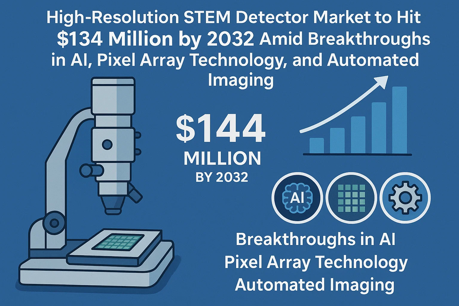
The global High-Resolution Scanning Transmission Electron Microscope (STEM) Detector Market is undergoing a transformative phase, powered by rapid technological advancements in imaging, automation, and detector hardware. According to industry estimates, the market was valued at US$ 89 million in 2024 and is expected to reach US$ 134 million by 2032, growing at a CAGR of 5.9% from 2025 to 2032. This growth reflects the rising demand for ultra-high-resolution imaging across materials science, semiconductor research, nanotechnology, and life sciences.
The Driving Force: New-Generation Detectors and Integration
1. Thermo Fisher’s Iliad System – A Leap Toward Multimodal (S)TEM
In 2024, Thermo Fisher Scientific introduced its Iliad (S)TEM platform at the European Microscopy Congress. This fully integrated system supports seamless switching between multiple analytical modes—imaging, spectroscopy, and diffraction—without the need for reconfiguration. The Iliad allows researchers to:
- Access atomic-scale resolution.
- Combine multimodal datasets in real time.
- Improve throughput and repeatability in materials analysis.
This innovation is seen as a cornerstone in STEM detector integration, pushing laboratories toward more automated, AI-assisted workflows.
AI and Automation Are Becoming the Backbone
2. AutomaTEM: The Rise of Autonomous STEM
In early 2024, a UK-led consortium unveiled AutomaTEM, an AI-powered automation solution developed in collaboration with Thermo Fisher and the University of Manchester. Scheduled to be deployed in 2025, AutomaTEM can:
- Identify and target hundreds of sample regions without manual input.
- Perform chemical mapping at atomic resolution.
- Adapt imaging parameters in real time based on sample characteristics.
The combination of AI and automation in this project points to a future where electron microscopy becomes fully autonomous, drastically improving efficiency while lowering operator skill requirements.
Pixel Array Detectors: A New Standard in Resolution and Range
3. Cornell’s Groundbreaking Pixel Array Detector
Researchers at Cornell University developed a solid-state pixel-array STEM detector offering unmatched capabilities:
- 1 millisecond frame capture.
- Dynamic range from 1 to 1,000,000 electrons per pixel.
- Simultaneous diffraction and phase data recording.
Such high-dynamic-range (HDR) performance allows for richer datasets per scan and facilitates magnetic field and strain mapping at previously inaccessible resolutions. These detectors are especially beneficial for 4D STEM, which demands high-speed, high-fidelity data collection.
Scaling Cryo-EM: Direct Electron’s DE‑64 Detector
The release of the Direct Electron DE‑64, an 8k × 8k direct detector, marks a milestone for high-throughput microscopy:
- With a resolution of 67 megapixels, it offers a massive field of view.
- Designed for cryo-electron microscopy and high-res STEM, it supports both biological and materials applications.
This technology greatly enhances data acquisition efficiency, especially in large-scale projects such as pharmaceutical screening and structural biology.
Hitachi’s HF5000 – Performance Meets Precision
Hitachi High-Tech introduced the HF5000, a 200 kV aberration-corrected hybrid microscope that supports TEM, STEM, and SEM capabilities. Key features include:
- Dual-windowless SDD EDS detectors with industry-leading solid angles.
- Advanced aberration correction that self-adjusts during imaging.
- High-sensitivity elemental analysis ideal for battery materials and semiconductors.
The HF5000 is a powerful example of a detector-integrated system that delivers exceptional performance across imaging modalities.
Market Growth: What’s Fueling the Surge?
Several factors are accelerating the high-resolution STEM detector market:
- Growing demand for nanotechnology and semiconductor miniaturization.
- Increased public and private funding for materials research.
- Emergence of AI-driven platforms that reduce the learning curve and operational costs.
- Rise in 4D STEM adoption, requiring ultra-fast, pixelated detectors with high dynamic range.
Regions like North America, Europe, and parts of Asia-Pacific (notably Japan and South Korea) are expected to lead the adoption curve, thanks to their robust R&D ecosystems and investments in electron microscopy infrastructure.
The Future of STEM Detection
The industry is moving toward systems that are:
- Automated and intelligent – powered by AI and machine learning.
- Modular and multimodal – enabling seamless integration of different analysis modes.
- Faster and broader – thanks to advances in pixelated sensor technology.
By 2032, high-resolution STEM detectors will not only be essential tools in academia and industry but will likely become fully autonomous instruments, capable of continuous analysis, learning from data, and optimizing imaging strategies in real time.
The global High-Resolution STEM Detector Market is transitioning from incremental improvements to revolutionary shifts in capability. With strong tailwinds from AI, dynamic pixel array detectors, and cross-platform integration, the market is poised to reach US$ 134 million by 2032—a figure that may be exceeded if current trends in automation and semiconductor research continue to accelerate.
Laboratories that adopt these next-gen detectors will be better positioned to tackle the complex challenges of modern materials science, nanotechnology, and structural biology in an increasingly competitive research environment.
Comments (0)